ALLPCB


If you're an engineer or designer looking for reliable solutions to prototype complex circuit boards, 8-layer PCB prototyping services offer the speed and precision you need. These services ensure fast turnaround times, thorough design validation, and robust testing to bring your ideas to life. At ALLPCB, we specialize in delivering high-quality 8-layer PCB quick turn solutions, including design verification, DFM analysis, and testing services to meet tight deadlines and strict performance standards.
In this comprehensive guide, we’ll dive into the world of 8-layer PCB prototyping, exploring why these boards are critical for modern electronics, how fast turnaround impacts project timelines, and the importance of design validation. Whether you're working on telecommunications, medical devices, or high-speed computing, this blog will provide actionable insights to streamline your prototyping process.
Why Choose 8-Layer PCBs for Your Next Project?
8-layer PCBs are a go-to choice for advanced electronic designs that require high density, improved signal integrity, and compact layouts. Unlike simpler 2-layer or 4-layer boards, an 8 layer PCB offers multiple layers for routing power, ground, and signal traces, making it ideal for applications with complex circuitry. These boards are often used in industries like aerospace, automotive, and IoT, where performance and reliability are non-negotiable.
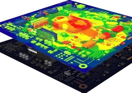
With eight layers, you can separate high-speed signals from power planes, reducing electromagnetic interference (EMI) and crosstalk. For instance, in a high-speed design operating at frequencies above 1 GHz, an 8-layer PCB allows for dedicated ground planes to maintain signal integrity, ensuring data rates remain stable. This level of control is critical for applications like 5G devices or high-performance computing systems.
The Importance of Fast Turnaround in 8-Layer PCB Prototyping
Time is often the most critical factor in product development. Delays in prototyping can push back entire project timelines, costing both time and money. This is where 8-layer PCB quick turn services shine. By leveraging advanced manufacturing processes and streamlined workflows, quick turn prototyping can deliver functional boards in as little as 24 to 48 hours for urgent needs.
Fast turnaround doesn't mean sacrificing quality. Modern prototyping services prioritize precision, ensuring that even with expedited schedules, your 8-layer PCB meets exact specifications. For example, if you're developing a prototype for a medical device that must comply with strict regulatory standards, quick turn services can help you iterate designs rapidly while maintaining tight tolerances, such as trace widths down to 3 mils for high-density layouts.
Speed also enables faster feedback loops. If a design flaw is identified during testing, a quick turn service allows you to revise and receive a new prototype in days, not weeks. This agility is invaluable for staying ahead in competitive markets.
Design Validation: Ensuring Your 8-Layer PCB Performs as Expected
Before moving to full-scale production, validating your design is a crucial step. 8-layer PCB design verification ensures that your board functions as intended under real-world conditions. This process involves checking for issues like signal integrity, PCB thermal management, and impedance mismatches that could compromise performance.
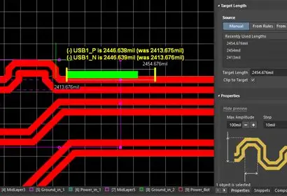
For high-speed designs, impedance control is a key focus during validation. If a trace on an 8-layer PCB has an impedance mismatch, it can cause signal reflections, leading to data errors. By using controlled impedance routing and verifying it with tools like Time-Domain Reflectometry (TDR), you can confirm that your board maintains a consistent 50-ohm impedance for critical signals. Design verification catches these problems early, saving costly redesigns later.
At ALLPCB, we integrate design validation into our prototyping process, offering detailed feedback on potential issues. This proactive approach ensures that your 8-layer PCB is ready for the next stage, whether it's further testing or production.
DFM Analysis: Optimizing Your 8-Layer PCB for Manufacturing
Design for Manufacturability (DFM) analysis is a critical step in 8-layer PCB prototyping. This process evaluates your design to ensure it can be manufactured efficiently without errors or unnecessary costs. With the complexity of an 8-layer board, which often includes fine-pitch components and microvias, overlooking DFM can lead to production delays or defective boards.
During 8-layer PCB DFM analysis, several factors are assessed, such as:
- Trace and Spacing: Ensuring that traces meet minimum width and spacing requirements (e.g., 4 mils for high-density designs) to avoid short circuits.
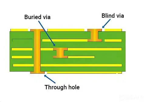
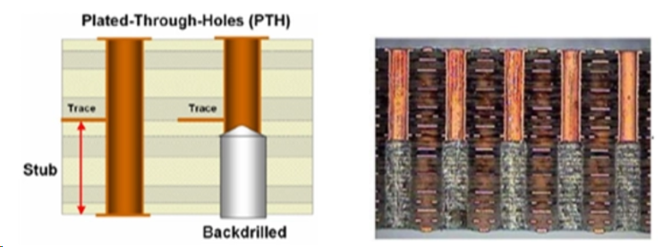
- Via Placement: Checking for proper placement of blind and buried vias, which are common in multilayer boards, to prevent drilling errors.
- Material Selection: Verifying that the chosen laminate and copper thickness (e.g., 1 oz or 2 oz copper) align with thermal and electrical needs.
By conducting DFM analysis early, potential issues like insufficient annular rings or overly tight tolerances can be addressed before fabrication begins. This not only speeds up the manufacturing process but also reduces the risk of costly rework. ALLPCB offers comprehensive DFM checks as part of our prototyping services, ensuring your design transitions smoothly from concept to reality.
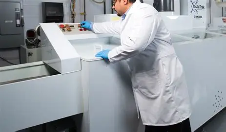
Testing Services: Guaranteeing Reliability of Your 8-Layer PCB
Testing is the final frontier in ensuring your 8-layer PCB meets performance and reliability standards. 8-layer PCB testing services cover a range of evaluations, from basic electrical continuity checks to advanced functional testing under simulated operating conditions.
Common tests include:
- In-Circuit Testing (ICT): Verifies that all components are correctly placed and soldered, checking for open or short circuits.
- Signal Integrity Testing: Measures how well high-speed signals travel across the board, ensuring minimal loss or distortion at frequencies like 2.5 GHz for modern applications.
- Thermal Stress Testing: Evaluates how the board handles heat dissipation, critical for power-intensive designs where layers may carry significant current.
For an 8-layer PCB used in automotive electronics, for instance, thermal testing might simulate temperature swings from -40°C to 85°C to confirm reliability in harsh environments. These rigorous tests ensure that your prototype can withstand real-world demands before moving to mass production.
ALLPCB provides a full suite of testing services tailored to 8-layer PCBs, giving you confidence that your design will perform as expected in its final application.
Benefits of Partnering with ALLPCB for 8-Layer PCB Prototyping
Choosing the right partner for your prototyping needs can make all the difference. At ALLPCB, we combine speed, precision, and expertise to deliver top-tier 8-layer PCB prototyping services. Here’s why engineers trust us:
- Rapid Turnaround: Our 8-layer PCB quick turn capabilities ensure you receive prototypes in record time, helping you meet tight deadlines.
- Comprehensive Validation: From design verification to DFM analysis, we scrutinize every detail to prevent issues down the line.
- Advanced Testing: Our 8-layer PCB testing services cover everything from electrical checks to environmental stress tests, ensuring reliability.
- Expert Support: Our team of engineers provides personalized guidance, helping you optimize your design for performance and manufacturability.
Whether you're iterating on a new product or preparing for production, our end-to-end services streamline the process, saving you time and resources.
Key Considerations When Prototyping 8-Layer PCBs
To ensure a successful prototyping phase, keep these factors in mind:
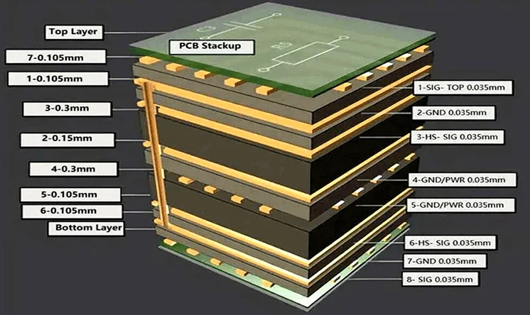
- Layer Stackup Planning: Design your stackup early to balance signal, power, and ground layers. A typical 8-layer stackup might include 4 signal layers and 4 ground/power planes for optimal EMI control.
- Component Placement: Place high-speed components strategically to minimize trace lengths, reducing signal delay and interference.
- Collaboration with Manufacturer: Share detailed design files and communicate specific requirements (e.g., impedance targets of 50 ohms) to avoid missteps during fabrication.
By addressing these elements upfront, you can avoid common pitfalls and ensure your 8-layer PCB prototype meets both functional and manufacturing goals.
How Fast Turnaround and Validation Impact Time-to-Market
In today’s fast-paced electronics industry, getting your product to market quickly is a competitive advantage. Fast turnaround prototyping for 8-layer PCBs, combined with thorough design validation, significantly shortens development cycles. For example, if a design iteration typically takes two weeks with traditional prototyping, a quick turn service can cut that down to 48 hours, allowing multiple revisions in the same timeframe.
Validation further accelerates the process by identifying flaws early. If a signal integrity issue is caught during design verification, you can fix it before fabrication, avoiding the expense of scrapping faulty boards. Together, these practices ensure your product moves from concept to market with minimal delays.
Conclusion: Streamline Your 8-Layer PCB Prototyping with ALLPCB
Prototyping 8-layer PCBs is a complex but essential step in developing cutting-edge electronics. With the right approach to fast turnaround, design validation, DFM analysis, and testing, you can ensure your project stays on track and meets the highest standards of performance. ALLPCB is committed to supporting engineers with top-notch 8-layer PCB prototyping services, helping you navigate the challenges of multilayer designs with ease.
From quick turn delivery to comprehensive testing services, we provide the tools and expertise needed to bring your vision to life. Start your next project with confidence, knowing that every detail of your 8-layer PCB will be meticulously handled for optimal results.