 ALLPCB


In-flight entertainment (IFE) systems are a critical part of modern aerospace design, ensuring passengers stay engaged during long flights. However, the performance of these systems heavily depends on the printed circuit board (PCB) design, especially the layer stackup. So, how do you optimize a PCB layer stackup for IFE systems? The key lies in strategic signal layer placement, effective ground plane design, and ensuring signal integrity under the unique constraints of aerospace environments. In this blog, we’ll dive deep into the essentials of aerospace PCB stackup design, offering practical tips and insights to enhance performance for IFE applications.
Why PCB Layer Stackup Matters for In-Flight Entertainment Systems
IFE systems, which include video displays, audio outputs, and connectivity modules, operate in a challenging environment. They must handle high-speed data, resist electromagnetic interference (EMI), and function reliably under extreme conditions like temperature fluctuations and vibrations. A well-optimized PCB layer stackup is the foundation for meeting these demands. It directly impacts signal integrity, power distribution, and noise reduction—all crucial for delivering seamless entertainment to passengers.
A poorly designed stackup can lead to issues like crosstalk between signal layers, power supply noise, or even system failures. For aerospace applications, where safety and reliability are non-negotiable, optimizing the PCB layer stackup isn’t just a good practice—it’s a necessity. Let’s explore how to achieve this with a focus on signal layer placement and ground plane design.
Understanding PCB Layer Stackup Basics
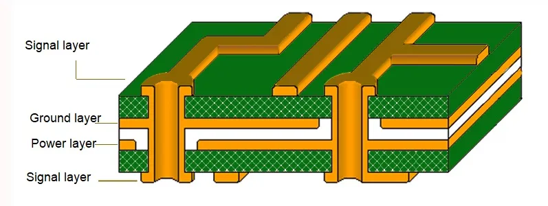
Before diving into optimization techniques, let’s cover the basics of PCB layer stackup. A stackup refers to the arrangement of conductive and insulating layers in a PCB. These layers typically include signal layers for data transmission, power planes for voltage distribution, and ground planes for noise reduction. The number of layers can vary—common configurations for IFE systems range from 4 to 16 layers, depending on complexity.
In aerospace PCB stackup design, every layer’s position and purpose must be carefully planned. For instance, placing signal layers too close without a ground plane in between can cause interference. Similarly, improper power and ground plane placement can lead to voltage drops or uneven current distribution. With IFE systems often handling high-speed signals (up to several gigabits per second for video streaming), a strategic stackup is vital for maintaining performance.
Key Factors in Aerospace PCB Stackup for IFE Systems
Optimizing a PCB layer stackup for in-flight entertainment involves addressing several critical factors unique to aerospace environments. Here are the main considerations:
1. Signal Integrity with High-Speed Data
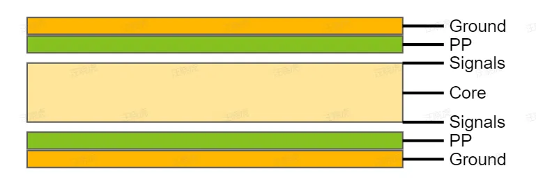
IFE systems transmit large amounts of data, such as high-definition video streams or real-time connectivity updates. High-speed signals, often exceeding 5 Gbps, require controlled impedance to prevent signal degradation. Impedance mismatches can cause reflections, leading to data errors or delays. To maintain signal integrity, signal layers should be placed adjacent to a reference plane (usually a ground plane) to provide a consistent return path. For example, in a 6-layer PCB, a common stackup might be:
- Layer 1: Signal (Top)
- Layer 2: Ground Plane
- Layer 3: Signal
- Layer 4: Power Plane
- Layer 5: Ground Plane
- Layer 6: Signal (Bottom)
This configuration ensures that each signal layer has a nearby ground plane, minimizing loop inductance and reducing noise. Tools like impedance calculators can help target specific values, such as 50 ohms for single-ended traces or 100 ohms for differential pairs, which are common in high-speed designs.
2. Electromagnetic Interference (EMI) Control
Aerospace environments are prone to EMI due to the presence of multiple electronic systems in close proximity. EMI can disrupt IFE performance, causing glitches or complete system failures. A well-designed ground plane in the PCB stackup acts as a shield, absorbing stray electromagnetic fields and providing a low-impedance return path for signals. Continuous ground planes are preferred over split planes, as splits can create unintended antennas, worsening EMI issues.
For IFE systems, it’s best to dedicate entire layers to ground planes and avoid routing signals through them. This approach not only reduces EMI but also enhances thermal management by distributing heat evenly across the board.
3. Power Distribution and Stability
Power integrity is another crucial aspect of aerospace PCB stackup design. IFE systems often require multiple voltage levels to power different components, such as 3.3V for digital circuits and 12V for display backlighting. Voltage drops or noise on power lines can lead to erratic system behavior. To address this, power planes should be placed close to ground planes to minimize loop area and reduce noise coupling. Adding decoupling capacitors near power pins can further stabilize voltage levels.
In a typical 8-layer stackup for IFE systems, power and ground layers might alternate with signal layers to ensure balanced distribution:
- Layer 1: Signal
- Layer 2: Ground
- Layer 3: Power (3.3V)
- Layer 4: Signal
- Layer 5: Signal
- Layer 6: Power (12V)
- Layer 7: Ground
- Layer 8: Signal
This arrangement helps maintain clean power delivery while isolating high-speed signals from power-related noise.
4. Mechanical and Environmental Constraints
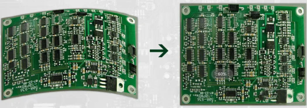
Aerospace environments impose strict mechanical and environmental demands on PCB designs. IFE systems must withstand vibrations during takeoff and landing, as well as temperature swings from -40°C to 85°C. The PCB stackup must use materials with low thermal expansion coefficients, such as high-Tg FR4 or polyimide, to prevent delamination or cracking. Additionally, the stackup should balance layer thickness to avoid warping under stress. For instance, a symmetrical stackup (equal dielectric thickness on both sides of the core) helps maintain structural integrity.
Best Practices for Signal Layer Placement in IFE PCB Stackups
Signal layer placement is a cornerstone of optimizing PCB performance for IFE systems. Improper placement can lead to crosstalk, signal delays, or increased EMI. Here are some best practices to follow:
- Isolate High-Speed Signals: Place high-speed signal layers (e.g., for HDMI or USB data) near ground planes to provide a stable reference and minimize crosstalk. Avoid placing two high-speed signal layers directly adjacent to each other without a separating ground plane.
- Prioritize Critical Signals: Route critical signals, such as clock lines or differential pairs, on outer layers if possible. Outer layers offer better control over trace width and spacing for impedance matching.
- Minimize Layer Transitions: Excessive via transitions between layers can introduce signal delays and reflections. Plan the stackup to keep related signals on the same layer or adjacent layers to reduce via usage.
For example, in a 4-layer PCB design for a simpler IFE module, an effective stackup could be:
- Layer 1: Signal (High-Speed Data)
- Layer 2: Ground
- Layer 3: Power
- Layer 4: Signal (Control Lines)
This setup ensures high-speed signals on Layer 1 have a direct reference to the ground plane on Layer 2, reducing noise and maintaining signal integrity.
Ground Plane PCB Design: The Backbone of Noise Reduction
A robust ground plane design is essential for any aerospace PCB stackup, especially for IFE systems where noise can degrade user experience. Here’s how to optimize ground planes:
- Use Continuous Ground Planes: Avoid splitting ground planes unless absolutely necessary for isolating analog and digital sections. Splits can disrupt return paths, creating noise and EMI issues.
- Place Ground Planes Strategically: Position ground planes adjacent to signal layers to provide a low-impedance return path. In multilayer boards, dedicate at least one full layer to ground for maximum effectiveness.
- Stitch Vias for Ground Continuity: Use stitching vias to connect ground planes across layers, ensuring a consistent reference for signals. Space vias at intervals of about 1/10th of the wavelength of the highest frequency signal to prevent resonance.
For IFE systems, where frequencies can reach into the gigahertz range for data transmission, a solid ground plane design can reduce noise by up to 20 dB, significantly improving system reliability.
Advanced Tips for Aerospace PCB Stackup Optimization
Beyond the basics, here are some advanced strategies to further enhance IFE PCB performance:
- Simulate Stackup Performance: Use simulation software to model signal integrity and EMI before fabrication. Tools can predict issues like crosstalk or impedance mismatches, allowing adjustments to layer spacing or dielectric materials. For instance, a dielectric constant (Dk) of 4.2 for FR4 material might be adjusted to a lower Dk for faster signal propagation.
- Consider Hybrid Stackups: For complex IFE systems, hybrid stackups combining different materials (e.g., FR4 for inner layers and high-frequency laminates for outer layers) can optimize performance. This approach balances cost with the need for high-speed signal handling.
- Optimize Layer Count: While more layers (e.g., 12 or 16) offer greater routing flexibility, they increase cost and complexity. Evaluate the minimum number of layers needed to meet signal and power requirements without over-engineering the design.
Common Mistakes to Avoid in IFE PCB Stackup Design
Even experienced engineers can make errors in PCB layer stackup design. Here are some pitfalls to steer clear of:
- Ignoring Symmetry: An asymmetrical stackup can lead to board warping under thermal stress, especially in aerospace environments. Always aim for balanced dielectric thickness across layers.
- Overloading Signal Layers: Packing too many traces on a single layer can cause crosstalk and routing congestion. Distribute signals across multiple layers with ground planes as separators.
- Neglecting Manufacturer Guidelines: Different fabrication processes have specific constraints on layer thickness and material options. Consult with your manufacturing partner early to ensure the stackup is producible.
Conclusion: Building Reliable IFE Systems with Optimized PCB Stackups
Optimizing the PCB layer stackup for in-flight entertainment systems is a complex but rewarding process. By focusing on signal layer placement, ground plane design, and the unique demands of aerospace environments, you can achieve superior performance and reliability. Whether it’s maintaining signal integrity for high-speed data or reducing EMI to ensure uninterrupted service, every detail in the stackup matters.
Start with a clear understanding of your system’s requirements, prioritize ground and power plane placement, and leverage simulation tools to fine-tune the design. With these strategies, your IFE PCBs will not only meet but exceed the rigorous standards of aerospace applications, delivering an exceptional passenger experience at 30,000 feet.


