ALLPCB


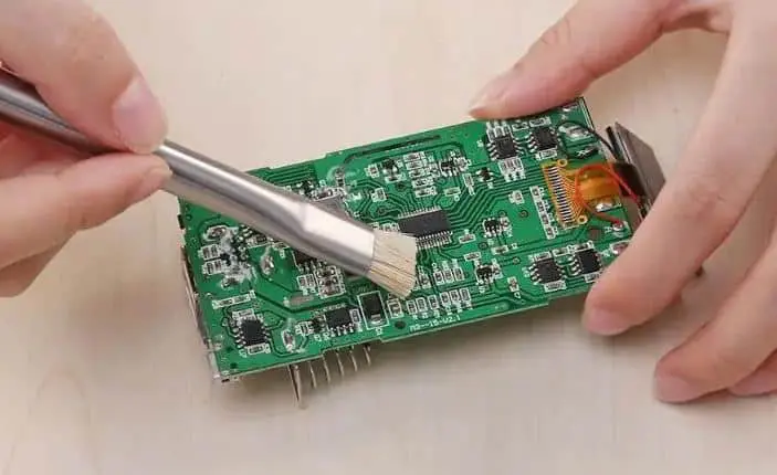
If you're an electrical engineer looking to perfect your understanding of the PCB lamination process, you're in the right place. PCB lamination is a critical step in manufacturing printed circuit boards, especially for multilayer designs. It involves bonding layers of materials together to create a strong, functional board. In this guide, we'll cover everything you need to know about PCB lamination materials, the step-by-step process, PCB lamination best practices, common defects, and troubleshooting tips. Whether you're working on a simple prototype or a complex multilayer PCB lamination project, this blog will help you achieve reliable results.
What Is PCB Lamination and Why Does It Matter?
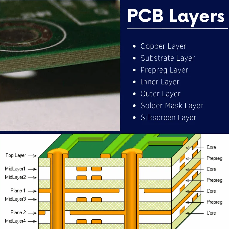
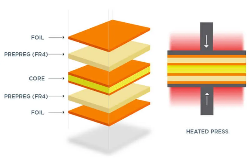
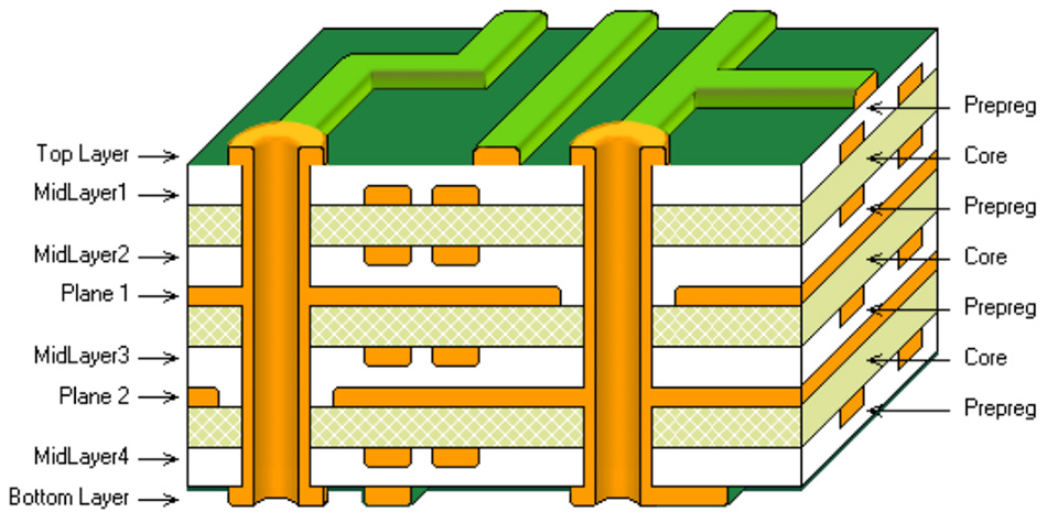
PCB lamination is the process of stacking and bonding multiple layers of materials—such as copper foil, prepreg (pre-impregnated resin sheets), and core laminates—using heat and pressure. This creates a single, unified structure that forms the foundation of a printed circuit board. For electrical engineers, understanding this process is essential because it directly impacts the board's electrical performance, mechanical strength, and long-term reliability.
In multilayer PCB lamination, the stakes are even higher. Missteps during lamination can lead to issues like delamination, poor signal integrity, or even complete board failure. With modern electronics demanding higher speeds (often exceeding 10 Gbps for high-speed signals) and tighter impedance control (typically targeting ±10% tolerance), getting lamination right is non-negotiable.
Understanding PCB Lamination Materials
The quality of a laminated PCB starts with the right PCB lamination materials. Each material plays a specific role in the board's performance. Here's a breakdown of the key components:
- Copper Foil: This conductive layer forms the circuit traces. Standard thicknesses range from 0.5 oz (17.5 μm) to 2 oz (70 μm) per square foot. The surface of the copper is often treated (e.g., with brown or black oxide) to improve adhesion during lamination.
- Prepreg: These are fiberglass sheets pre-impregnated with resin. Prepreg acts as the "glue" that bonds layers together. Common resin systems include epoxy, with dielectric constants (Dk) typically between 3.5 and 4.5 at 1 MHz, affecting signal speed and impedance.
- Core Laminate: This is the rigid base material, often made of woven fiberglass and epoxy resin. Core thickness can vary from 0.1 mm to 1.6 mm, depending on the design requirements.
- Specialty Materials: For high-frequency or high-temperature applications, materials like PTFE (Teflon) or polyimide may be used. These have lower Dk values (around 2.2 for PTFE) and better thermal stability (up to 260°C).
Choosing the right materials depends on your project's needs. For example, if you're designing a board for a 5G application, you might prioritize low-loss materials with a dissipation factor (Df) below 0.002 to minimize signal loss at frequencies above 10 GHz.
The PCB Lamination Process: Step by Step
The PCB lamination process is a precise operation that requires careful control of temperature, pressure, and time. Here's how it works for a typical multilayer board:
- Preparation of Layers: Inner layers are etched with circuit patterns and treated with an oxide process to roughen the copper surface for better adhesion. This step prevents delamination later on.
- Stacking: Layers of prepreg, core, and copper foil are carefully aligned and stacked. Registration holes or pins ensure precise alignment, critical for maintaining via connectivity in multilayer designs.
- Lamination: The stack is placed in a lamination press. Heat (typically 170-200°C) and pressure (around 200-400 psi) are applied for 60-120 minutes. This cures the resin in the prepreg, bonding the layers into a solid board.
- Cooling: The board is slowly cooled under pressure to prevent warping due to thermal stress. Rapid cooling can cause internal stresses, leading to defects.
- Inspection: Post-lamination, the board is checked for thickness (targeting ±10% of design specs), flatness, and initial signs of defects like voids or delamination.
For engineers, understanding these parameters is key to troubleshooting issues. For instance, if the lamination temperature is too low (below 160°C), the resin may not fully cure, resulting in weak bonds and potential delamination under thermal stress.
PCB Lamination Best Practices for Engineers
Following PCB lamination best practices can make the difference between a reliable board and a costly failure. Here are actionable tips tailored for electrical engineers:
- Material Selection: Match material properties to your design needs. For high-speed designs, choose low-Dk prepregs (e.g., 3.0-3.5) to maintain signal integrity. Check datasheets for thermal expansion coefficients (CTE) to avoid mismatch between layers, which can cause warping at temperatures above 150°C.
- Layer Alignment: Use optical alignment systems or X-ray inspection during stacking to ensure registration accuracy within 0.05 mm. Misalignment can lead to via failures, especially in boards with 0.1 mm microvias.
- Temperature and Pressure Control: Monitor lamination parameters closely. A temperature variation of just 5°C can affect resin flow, leading to voids. Use calibrated equipment to maintain consistency.
- Prepreg Storage: Store prepreg in a cool, dry environment (below 23°C and 50% humidity) to prevent moisture absorption, which can cause blisters during lamination.
- Post-Lamination Testing: Conduct microsection analysis to check for internal defects. Measure interlayer bonding strength (typically targeting >1.0 N/mm) to ensure reliability under thermal cycling (e.g., -40°C to 85°C for automotive applications).
By focusing on these practices, you can reduce the risk of failures and ensure your boards meet performance standards like IPC-6012 for qualification and performance.
Common PCB Lamination Defects and Their Causes
Even with the best preparation, PCB lamination defects can occur. Identifying these issues early saves time and resources. Here are the most common problems and their root causes:
- Delamination: This is the separation of layers, often caused by poor copper surface treatment (e.g., inadequate oxide roughening) or moisture in prepreg. Delamination can lead to open circuits or reduced mechanical strength.
- Voids: Air bubbles trapped between layers due to insufficient pressure or uneven resin flow. Voids can disrupt signal paths, especially in high-frequency boards operating above 5 GHz.
- Resin Starvation: Insufficient resin in prepreg fails to fill gaps, leading to weak bonds. This often happens if the lamination temperature is too high (above 210°C), causing premature curing.
- Warping: Uneven thermal expansion or cooling stress causes the board to bend. A CTE mismatch between materials (e.g., 15 ppm/°C for core vs. 50 ppm/°C for prepreg) is a common culprit.
- Resin Smear: Excess resin flows into via holes during lamination, blocking connections. This can occur if pressure is too high (above 500 psi) or if via holes are not properly cleaned before lamination.
These defects can compromise a board's performance, especially in critical applications like aerospace or medical devices where failure rates must be below 0.01%.
PCB Lamination Troubleshooting: Practical Solutions
When defects occur, effective PCB lamination troubleshooting is essential. Here are practical steps to diagnose and fix common issues:
- Delamination Issues: Check copper surface preparation. If oxide treatment is uneven, reprocess inner layers with a consistent black or brown oxide layer (targeting 1-2 μm thickness). Also, verify prepreg storage conditions—moisture content should be below 0.5%.
- Voids in Layers: Increase lamination pressure by 10-20 psi and extend heating time by 10-15 minutes to improve resin flow. Use vacuum lamination presses to remove trapped air, reducing void incidence by up to 30%.
- Resin Starvation: Select prepreg with higher resin content (e.g., 50-60%) for complex designs. Lower lamination temperature by 5-10°C to prevent early curing and ensure complete gap filling.
- Warping Problems: Balance the stack-up design by ensuring symmetrical layer distribution. If warping persists, adjust cooling rates to below 2°C per minute to minimize thermal stress.
- Resin Smear in Vias: Reduce lamination pressure to below 350 psi and ensure vias are debris-free before stacking. Post-lamination drilling can also clean out minor smear, though it risks via wall damage if not done precisely.
For engineers, documenting each troubleshooting step is critical. Keep a log of process parameters and defect rates to identify patterns. For instance, if delamination occurs repeatedly in boards laminated above 200°C, you might need to adjust your equipment calibration or material specs.
Special Considerations for Multilayer PCB Lamination
Multilayer PCB lamination introduces additional complexity due to the increased number of layers (often 4 to 16 or more) and tighter design constraints. Here are key points to consider:
- Signal Integrity: With multilayer boards, maintaining impedance control (e.g., 50 ohms for single-ended traces) is critical. Use consistent dielectric thicknesses (within ±0.05 mm) to avoid signal reflections at speeds above 1 Gbps.
- Thermal Management: More layers mean higher heat generation. Select materials with low CTE (below 20 ppm/°C) to prevent cracking during thermal cycling in applications like automotive electronics.
- Via Reliability: Ensure precise drill registration (within 0.025 mm) to avoid misaligned vias, which can cause open circuits. Blind and buried vias in multilayer designs are especially vulnerable to lamination stress.
Multilayer boards often power cutting-edge tech, from 5G infrastructure to AI hardware. A single lamination error can delay a project by weeks, so invest time in simulation tools like Altium or Cadence to predict stack-up behavior before fabrication.
Conclusion: Elevate Your PCB Lamination Skills
Mastering the PCB lamination process is a game-changer for electrical engineers. By understanding PCB lamination materials, following PCB lamination best practices, and knowing how to tackle PCB lamination defects through effective PCB lamination troubleshooting, you can ensure your boards meet the highest standards of performance and reliability. Whether you're focused on multilayer PCB lamination or a simpler design, attention to detail during lamination pays off in reduced failures and faster time-to-market.
Start by reviewing your current process. Are your materials optimized for your application? Are you monitoring lamination parameters closely? Use the tips and insights from this guide to refine your approach. If you've encountered unique lamination challenges, share your experiences in the comments—we'd love to hear how you've solved them!
With the right knowledge and practices, you can turn PCB lamination from a potential pain point into a strength of your engineering toolkit. Keep learning, keep testing, and keep building better boards.