ALLPCB


In the world of printed circuit board (PCB) design, achieving optimal PCB signal integrity is a top priority for engineers working on high-speed applications. One often-overlooked factor that plays a critical role in maintaining signal quality is line width tolerance. But what exactly is line width tolerance, and why does it matter? Simply put, it refers to the acceptable variation in the width of a PCB trace during manufacturing. Even small deviations in trace width variation can lead to issues like signal reflection and impedance mismatch, disrupting the performance of transmission lines. In this blog, we’ll dive deep into the importance of line width tolerance, how it impacts signal integrity, and practical steps to manage it effectively for reliable PCB designs.
What Is Line Width Tolerance and Why Does It Matter?
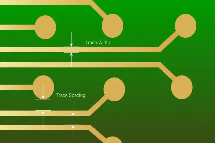
Line width tolerance is the range within which the actual width of a PCB trace can vary from its designed value during the manufacturing process. For example, if a trace is designed to be 5 mils wide, a tolerance of ±10% means the actual width could range between 4.5 and 5.5 mils. While this might seem like a minor deviation, it can have a significant impact on high-speed designs where precision is critical.
In high-frequency circuits, the width of a trace directly affects its impedance—a measure of opposition to the flow of alternating current. When trace width variation occurs outside the acceptable tolerance, it can cause an impedance mismatch, leading to signal reflection. These reflections can distort signals, introduce noise, and degrade the overall performance of the PCB. For applications like telecommunications, automotive electronics, and data centers, where signal integrity is non-negotiable, controlling line width tolerance becomes essential.
How Trace Width Variation Impacts PCB Signal Integrity
Signal integrity refers to the ability of a signal to travel through a PCB without distortion or loss of quality. When trace width varies beyond the specified tolerance, several issues can arise that compromise this integrity. Let’s explore the key effects in detail.
1. Impedance Mismatch and Signal Reflection
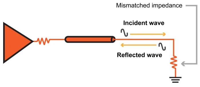
Impedance is a critical parameter in transmission lines, especially for high-speed digital and RF circuits. The impedance of a trace depends on its width, thickness, and the dielectric properties of the PCB material. A standard target impedance for many high-speed designs is 50 ohms, but even a small variation in trace width—say, from 5 mils to 4.5 mils—can change this value by several ohms. This creates an impedance mismatch, causing part of the signal to reflect back toward the source instead of reaching its destination.
These reflections can lead to signal distortion, increased jitter, and even data errors in digital systems operating at speeds above 1 GHz. For instance, in a DDR4 memory interface running at 2.4 Gbps, a mere 5% deviation in trace width could result in enough reflection to cause bit errors, impacting system reliability.
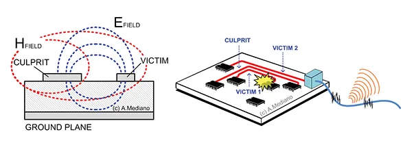
2. Crosstalk and Electromagnetic Interference (EMI)
Uneven trace widths can also exacerbate crosstalk—the unwanted coupling of signals between adjacent traces. When one trace is narrower than designed, the spacing between it and a neighboring trace effectively increases, altering the electromagnetic field distribution. This can lead to higher EMI, which interferes with nearby circuits and degrades PCB signal integrity. In sensitive applications like medical devices, such interference could have serious consequences.
3. Signal Delay and Timing Issues
In high-speed designs, signal timing is crucial. Variations in trace width can cause slight differences in signal propagation delay across different parts of the board. For example, a wider trace might have a lower resistance and slightly faster signal travel time compared to a narrower one. Over long distances, these tiny delays add up, causing skew in differential pairs and timing mismatches in clock signals. This is particularly problematic in systems like USB 3.0, where signal speeds reach up to 5 Gbps, and timing precision is vital.
The Role of Manufacturing in Line Width Tolerance
Line width tolerance isn’t just a design concern—it’s heavily influenced by the manufacturing process. During PCB fabrication, factors like etching accuracy, copper thickness, and material uniformity can lead to trace width variation. Let’s break down how these factors play a role and what designers can do to mitigate their impact.
Etching Precision
The etching process removes unwanted copper from the PCB to form traces. However, over-etching or under-etching can result in traces that are narrower or wider than intended. Modern manufacturing processes can achieve tolerances as tight as ±10%, but for high-speed designs, even this level of variation might be too much. Collaborating with a manufacturer that uses advanced etching techniques and quality control measures can help maintain tighter tolerances, often down to ±5% for critical applications.
Copper Thickness Variations
The thickness of the copper layer also affects trace impedance. If the copper is thicker than specified, the trace might end up narrower after etching to achieve the desired resistance, leading to unexpected impedance values. Standard copper thicknesses like 1 oz/ft2 (approximately 35 μm) are common, but variations of even 10% can impact high-frequency signals. Specifying precise copper weights and verifying them during production can reduce this risk.
Material Consistency
The dielectric constant of the PCB substrate material, such as FR-4, influences impedance alongside trace width. If the material’s properties vary across the board, it can compound the effects of trace width deviations. Using high-quality laminates with consistent dielectric properties is a practical step to minimize such issues.
Strategies to Manage Line Width Tolerance for Better Signal Integrity
Maintaining tight line width tolerance is a team effort between designers and manufacturers. Here are actionable strategies to ensure PCB signal integrity by controlling trace width variation.
1. Design with Tolerance in Mind
Start by designing traces with realistic tolerances based on manufacturing capabilities. For instance, if your manufacturer can achieve a ±10% tolerance, avoid designing traces at the extreme edge of this range where variations could push impedance out of spec. Use impedance calculators during the design phase to simulate how a 10% variation in width affects your target impedance (e.g., 50 ohms for RF signals). Adjust trace widths and spacing accordingly to stay within safe limits.
2. Specify Controlled Impedance
For high-speed designs, specify controlled impedance traces in your design files. This means defining not just the trace width but also the target impedance value and acceptable tolerance. Many modern design tools allow you to input these parameters and generate stack-up configurations that account for manufacturing variations. Communicate these requirements clearly to your manufacturer to ensure they prioritize precision during fabrication.
3. Use Wider Traces for Less Sensitivity
In some cases, using slightly wider traces can reduce the impact of width variations. A wider trace has a lower percentage change in impedance for the same absolute variation. For example, a 10% variation on a 5-mil trace changes its width by 0.5 mils, while the same percentage on a 10-mil trace changes it by 1 mil—but the relative impact on impedance is smaller for the wider trace. Balance this approach with board space constraints and signal routing needs.
4. Collaborate with Your Manufacturer
Work closely with your PCB manufacturer to understand their process capabilities and limitations. Request test coupons—small test structures on the PCB panel that measure actual trace widths and impedance after fabrication. These coupons can help verify whether the manufactured board meets your tolerance specifications before full assembly. For critical projects, consider opting for premium fabrication services that offer tighter tolerances, even if they come at a higher cost.
5. Simulate and Test for Signal Integrity
Before finalizing your design, use simulation tools to model the effects of trace width variations on signal reflection and impedance mismatch. Tools like SPICE or field solvers can predict how a ±10% variation impacts signal behavior at frequencies above 1 GHz. After manufacturing, perform signal integrity testing using oscilloscopes or time-domain reflectometry (TDR) to measure actual impedance and identify any reflections caused by width deviations.
Real-World Applications: Why Line Width Tolerance Matters
The importance of line width tolerance becomes even clearer when we look at real-world applications. In 5G telecommunications, for instance, signal frequencies often exceed 20 GHz, making even minor variations in trace width a potential cause of signal loss or reflection. A study in high-speed PCB design found that a 5% deviation in trace width at 10 GHz can increase return loss by up to 3 dB, significantly degrading performance.
Similarly, in automotive electronics, where systems like advanced driver-assistance systems (ADAS) rely on precise timing, trace width variations can introduce delays that affect sensor data transmission. Ensuring tight tolerances during design and manufacturing can prevent such issues, leading to safer and more reliable vehicles.
Conclusion: Prioritizing Line Width Tolerance for PCB Success
In the fast-paced world of electronics, maintaining PCB signal integrity is more important than ever. Line width tolerance may seem like a small detail, but its impact on trace width variation, signal reflection, impedance mismatch, and the performance of transmission lines cannot be overstated. By understanding how manufacturing processes affect trace width, designing with realistic tolerances, and collaborating closely with manufacturers, engineers can minimize variations and ensure reliable signal transmission.
Whether you’re working on a high-speed digital circuit or an RF application, paying attention to line width tolerance is a crucial step toward building robust and efficient PCBs. Take the time to simulate, test, and refine your designs, and you’ll see the difference in performance and reliability. At ALLPCB, we’re committed to supporting your projects with high-quality fabrication services that prioritize precision and signal integrity every step of the way.