 ALLPCB


When it comes to choosing the right surface finish for printed circuit boards (PCBs), the decision between Electroless Nickel Immersion Gold (ENIG) and Hard Gold Plating can significantly impact performance, durability, and cost. If you're wondering which one is better for your project, the answer depends on your specific application. ENIG is often preferred for its excellent solderability and corrosion resistance, making it ideal for most general-purpose PCBs. On the other hand, Hard Gold Plating shines in high-wear applications like edge connectors due to its superior durability and resistance to friction. In this comprehensive guide, we’ll break down the ENIG vs Hard Gold comparison, exploring their advantages, disadvantages, and best use cases to help you make an informed decision.
Introduction to PCB Surface Finishes
A PCB surface finish is a critical layer applied to the copper traces of a circuit board to protect them from oxidation, ensure solderability, and enhance overall reliability. Without a proper finish, copper can corrode quickly when exposed to air, leading to poor connections and potential failures. The choice of surface finish affects not just the board’s functionality but also its manufacturing cost and longevity.
Two popular options in the industry are ENIG and Hard Gold Plating. Both involve a layer of gold to protect the underlying metal, but they differ in application methods, composition, and performance characteristics. This PCB surface finish comparison will dive deep into these two finishes, helping engineers and designers understand their strengths and weaknesses.
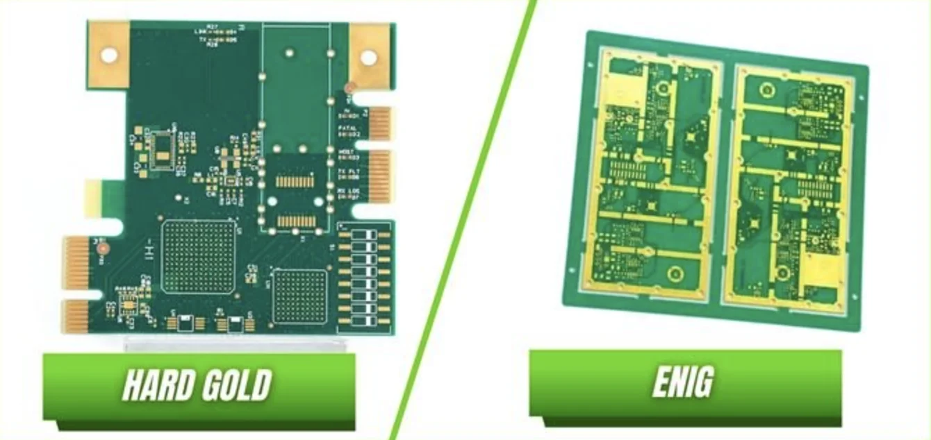
What is Electroless Nickel Immersion Gold (ENIG)?
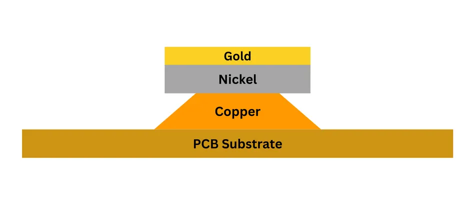
ENIG, or Electroless Nickel Immersion Gold, is a two-layer surface finish consisting of a nickel base layer and a thin gold top layer. The nickel layer, typically 3-6 micrometers thick, acts as a barrier to prevent copper diffusion and provides structural support. The gold layer, usually 0.05-0.1 micrometers thick, protects the nickel from oxidation and ensures excellent solderability.
The process of applying ENIG is chemical, meaning it doesn’t require an electric current. This electroless method allows for uniform deposition, even on complex board designs with fine-pitch components. ENIG is widely used in applications requiring reliable soldering, such as consumer electronics, telecommunications, and medical devices.
ENIG Advantages
- Excellent Solderability: The gold layer ensures strong and reliable solder joints, making ENIG ideal for surface-mount technology (SMT) and fine-pitch components.
- Corrosion Resistance: The nickel layer provides a robust barrier against oxidation, extending the shelf life of the PCB.
- Flat Surface: ENIG creates a smooth, even surface, which is critical for precise component placement and high-density designs.
- Cost-Effective for Most Applications: Compared to other gold-based finishes, ENIG is relatively affordable, especially for large-scale production.
- Lead-Free Compliance: ENIG meets RoHS standards, making it suitable for environmentally conscious designs.
ENIG Disadvantages
- Limited Durability for High-Wear Areas: The thin gold layer can wear off under repeated mechanical stress, making ENIG unsuitable for applications like edge connectors.
- Black Pad Issue: A potential defect known as "black pad" can occur due to improper nickel deposition, leading to weak solder joints and reliability issues.
- Not Ideal for High-Frequency Signals: The nickel layer can cause signal loss in high-frequency applications due to its magnetic properties, impacting performance at frequencies above 1 GHz.
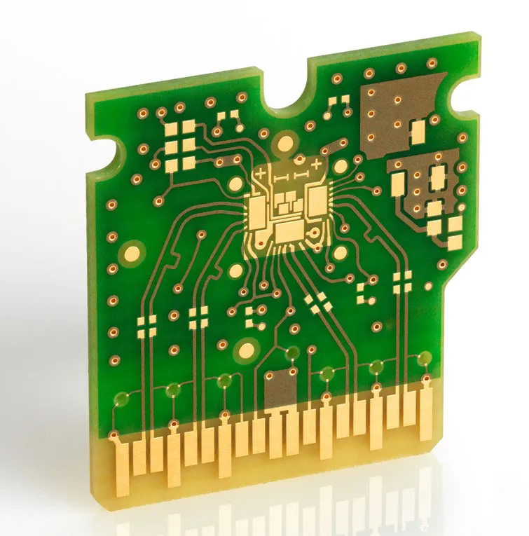
What is Hard Gold Plating?
Hard Gold Plating, also known as electrolytic gold plating, involves a thicker layer of gold (typically 0.8-2.5 micrometers) over a nickel underlayer (around 3-6 micrometers). Unlike ENIG, this process uses an electric current to deposit the gold, allowing for greater control over thickness. The gold in Hard Gold Plating is alloyed with other metals like cobalt or nickel to increase its hardness, making it extremely durable.
This finish is commonly used in areas of the PCB that experience frequent mechanical contact, such as edge connectors, test points, and keypads. Hard Gold Plating is often applied selectively to specific areas rather than the entire board to manage costs.
Hard Gold Plating Advantages
- Superior Durability: The thicker, harder gold layer withstands repeated friction and wear, making it perfect for connectors and high-contact areas. It can endure over 1,000 insertion cycles without significant degradation.
- Excellent Conductivity: Hard Gold provides low contact resistance, ensuring reliable electrical connections even after prolonged use.
- Customizable Thickness: The electrolytic process allows manufacturers to adjust the gold thickness based on specific requirements, offering flexibility for different applications.
- Resistance to Tarnishing: The gold layer resists oxidation and maintains its appearance and functionality over time.
Hard Gold Plating Disadvantages
- Higher Cost: The thicker gold layer and the electrolytic process make Hard Gold Plating more expensive than ENIG, especially for larger areas.
- Poor Solderability: Hard Gold is not ideal for soldering because the alloyed gold can create brittle joints, leading to potential failures.
- Selective Application Required: Due to cost, Hard Gold is often applied only to specific areas, which can complicate the manufacturing process.
- Porosity at Thin Layers: If the gold layer is too thin, it may develop pores, allowing the nickel underneath to oxidize and reducing reliability.
ENIG vs Hard Gold: A Detailed PCB Surface Finish Comparison
Now that we’ve covered the basics, let’s compare ENIG and Hard Gold Plating across several key factors to help you decide which is best for your project. This ENIG vs Hard Gold analysis focuses on performance, cost, and application suitability.
1. Solderability
ENIG excels in solderability thanks to its thin, pure gold layer, which ensures strong, reliable joints for SMT components. It’s a go-to choice for most modern PCBs where soldering is a primary concern. Hard Gold, however, is less suitable for soldering due to its alloyed composition, which can lead to brittle connections. If your design involves a lot of soldered components, ENIG is the better option.
2. Durability and Wear Resistance
Hard Gold Plating is the clear winner when it comes to durability. Its thicker, harder gold layer can withstand significant mechanical stress, making it ideal for edge connectors and test points that experience frequent contact. ENIG, with its thinner gold layer, cannot match this level of wear resistance and is better suited for static applications.
3. Cost Considerations
Cost is often a deciding factor in PCB manufacturing. ENIG is generally more affordable because it uses a thinner gold layer and a simpler chemical process. Hard Gold Plating, with its thicker gold and electrolytic application, is more expensive, especially if applied to large areas. However, its selective application can help manage costs in designs where only specific areas need high durability.
4. Application Suitability
The choice between ENIG and Hard Gold often comes down to the specific needs of your PCB. For general-purpose boards with soldered components, ENIG is typically sufficient and cost-effective. For applications requiring frequent mechanical contact, such as connectors in industrial equipment or consumer devices, Hard Gold is the preferred choice. Some designs even combine both finishes, using ENIG for solderable areas and Hard Gold for high-wear zones.
5. Signal Integrity for High-Frequency Designs
In high-frequency applications, signal integrity is critical. ENIG’s nickel layer can introduce signal loss due to its magnetic properties, making it less ideal for designs operating above 1 GHz. Hard Gold, while better in some respects, is rarely used across entire boards for high-frequency applications due to cost. If signal integrity is a primary concern, other finishes like immersion silver might be considered, though they fall outside this comparison.
When to Choose ENIG?
ENIG is the right choice for a wide range of applications, especially when solderability and cost are top priorities. Consider using ENIG if your project involves:
- High-density PCB designs with fine-pitch components.
- Consumer electronics, telecommunications, or medical devices.
- Lead-free soldering processes to comply with environmental regulations.
- Budget constraints that require a cost-effective yet reliable finish.
However, be cautious of potential issues like black pad defects, and ensure your manufacturing partner follows strict quality control measures to avoid such problems.
When to Choose Hard Gold Plating?
Hard Gold Plating is the go-to option for applications where durability under mechanical stress is essential. Opt for Hard Gold if your design includes:
- Edge connectors or test points that will experience frequent insertion and removal.
- Industrial equipment or devices requiring long-term reliability in harsh conditions.
- Areas needing low contact resistance for consistent electrical performance.
Keep in mind that Hard Gold is more expensive and less suitable for soldering, so it’s often used selectively alongside another finish like ENIG.
Combining ENIG and Hard Gold in Hybrid Designs
In some cases, you don’t have to choose between ENIG and Hard Gold—you can use both. Hybrid designs apply ENIG to solderable areas for cost-effective, reliable joints and Hard Gold to high-wear areas like connectors for durability. This approach balances performance and cost, though it may increase manufacturing complexity due to the need for multiple finishing processes.
For example, a PCB for a networking device might use ENIG across most of the board for component soldering, while the edge connectors feature Hard Gold to handle frequent plugging and unplugging. This tailored approach ensures optimal performance where it’s needed most.
Conclusion: Which Surface Finish Reigns Supreme?
In the battle of ENIG vs Hard Gold, there’s no universal winner—each surface finish has its unique strengths and weaknesses. ENIG stands out for its solderability, corrosion resistance, and affordability, making it a versatile choice for most PCB applications. Hard Gold Plating, with its unmatched durability and wear resistance, is indispensable for high-contact areas like edge connectors but comes at a higher cost and with limitations in soldering.
Ultimately, the best choice depends on your project’s specific requirements. Evaluate factors like mechanical stress, soldering needs, signal integrity, and budget to determine the right finish. By understanding the ENIG advantages, ENIG disadvantages, Hard Gold Plating advantages, and Hard Gold Plating disadvantages, you can make a decision that ensures reliability and performance for your PCB design.
At ALLPCB, we’re committed to helping you navigate these choices with expert guidance and high-quality manufacturing services. Whether you opt for ENIG, Hard Gold, or a hybrid approach, we ensure precision and reliability in every board we produce. Explore our surface finish options to bring your designs to life with confidence.


