 ALLPCB


In the world of PCB design, managing heat is a critical challenge. As electronic devices become smaller and more powerful, heat dissipation can make or break a product's performance and reliability. One effective solution for thermal management is the use of stacked vias. But when should you use stacked vias for optimal PCB heat dissipation? Simply put, stacked vias are ideal when you need to transfer heat efficiently across multiple layers of a PCB, especially in high-density or high-power designs where traditional thermal vias may not suffice. In this blog, we'll dive deep into the role of stacked vias in PCB thermal design, explore their benefits, and guide you on when and how to implement them for maximum heat dissipation.
Understanding PCB Thermal Management Challenges
Heat is an inevitable byproduct of electronic components in operation. Whether it's a high-performance processor, a power supply unit, or an LED driver, components generate heat that, if not managed properly, can lead to reduced performance, shortened lifespan, or even catastrophic failure. Effective thermal management ensures that heat is dissipated away from sensitive components to maintain optimal operating temperatures.
In PCB design, thermal management involves several strategies, such as using heat sinks, optimizing component placement, and incorporating thermal vias. While heat sinks help dissipate heat into the surrounding environment, thermal vias provide a direct path for heat to travel through the PCB layers to a heat sink or a ground plane. However, in complex multilayer designs, a single layer of thermal vias may not be enough to handle the heat load, which is where stacked vias come into play.
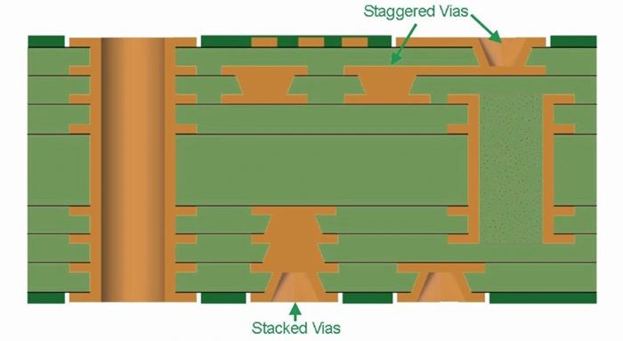
What Are Stacked Vias and How Do They Work?
Stacked vias are a specialized type of via structure in PCB design where multiple vias are aligned vertically across different layers of a multilayer board. Unlike standard thermal vias, which typically connect two adjacent layers, stacked vias create a continuous path through several layers, enhancing the thermal conductivity of the PCB. This design allows heat to be transferred more effectively from a heat-generating component on the top layer to a heat dissipation layer or heat sink on the bottom or internal layers.
The principle behind stacked vias is straightforward: they reduce thermal resistance by providing a shorter and more direct path for heat to travel. By stacking vias, you essentially create a "thermal highway" that can handle higher heat loads compared to a single via or a scattered array of vias. This is particularly useful in high-density designs where space is limited, and heat dissipation needs to be maximized without increasing the board's footprint.
For example, in a 6-layer PCB with a high-power component generating 10W of heat, a single layer of thermal vias might achieve a thermal resistance of 5°C/W. By using stacked vias across all layers, you could potentially reduce this to 2°C/W, significantly lowering the component's operating temperature.
Key Benefits of Stacked Vias in PCB Thermal Design
Stacked vias offer several advantages when it comes to thermal management in PCB design. Understanding these benefits can help you decide when to incorporate them into your projects.
- Enhanced Heat Transfer: Stacked vias provide a continuous low-resistance path for heat to travel through multiple layers, improving overall heat dissipation efficiency.
- Space Efficiency: In high-density designs, where board real estate is at a premium, stacked vias allow for effective heat management without requiring additional surface area.
- Improved Reliability: By reducing operating temperatures, stacked vias help prevent thermal stress on components, extending their lifespan and improving system reliability.
- Compatibility with Multilayer Designs: Stacked vias are particularly suited for complex multilayer PCBs, where heat needs to be transferred across several layers to reach a heat sink or ground plane.
When Should You Use Stacked Vias for Heat Dissipation?
Not every PCB design requires stacked vias. Their use depends on specific design constraints and thermal requirements. Here are some scenarios where stacked vias are the optimal choice for heat dissipation:
1. High-Power Components in Multilayer Boards
If your design includes high-power components such as power amplifiers, voltage regulators, or microprocessors on a multilayer PCB, stacked vias can efficiently channel heat away from these components. For instance, a component dissipating 15W of heat on a 10-layer board may cause a temperature rise of 50°C with standard vias. Stacked vias could reduce this rise to 30°C by improving heat transfer to a bottom-layer heat sink.
2. Limited Surface Area for Heat Sinks
In compact designs where there’s little room for large heat sinks or extensive copper pours, stacked vias offer a way to manage heat vertically through the board layers. This is common in portable devices or densely packed industrial control systems.
3. High-Density Interconnect (HDI) Designs
HDI PCBs often have multiple layers with fine traces and small vias. Stacked vias, which are typically microvias in HDI designs, can be used to create efficient thermal paths without compromising the board’s electrical performance.
4. Applications with Strict Thermal Limits
In industries like automotive or aerospace, components must operate within strict temperature ranges to ensure safety and reliability. Stacked vias help maintain these limits by providing robust heat dissipation in challenging environments.
5. Designs Requiring Internal Heat Dissipation Layers
Some PCBs are designed with internal copper planes dedicated to heat dissipation. Stacked vias are essential in these cases to connect heat-generating components on outer layers to these internal planes, ensuring effective thermal management.
Design Considerations for Implementing Stacked Vias
While stacked vias are a powerful tool for thermal management, their implementation requires careful planning. Here are some key considerations to keep in mind during PCB thermal design:
Via Placement and Density
Place stacked vias as close as possible to the heat source for maximum efficiency. The density of vias also matters—more vias mean better heat transfer, but too many can weaken the board’s structural integrity or interfere with signal routing. A common guideline is to use a grid of vias with a spacing of 0.3mm to 0.5mm under high-power components.
Material Selection
The thermal conductivity of the PCB material plays a role in heat dissipation. Standard FR-4 material has a thermal conductivity of about 0.3 W/m·K, which may not be sufficient for high-heat applications. Consider using high-thermal-conductivity materials like metal-core PCBs or laminates with better thermal properties (up to 1.0 W/m·K or higher) alongside stacked vias.
Via Fill and Plating
Stacked vias can be filled with thermally conductive materials like epoxy or copper to further reduce thermal resistance. Copper-filled vias, for example, can improve thermal conductivity by up to 30% compared to unfilled vias. Ensure proper plating thickness (typically 1oz or 2oz copper) to handle the thermal load.
Balancing Thermal and Electrical Needs
While stacked vias are great for heat dissipation, they can impact signal integrity if placed near high-speed traces. Work with simulation tools to balance thermal and electrical performance, ensuring that vias don’t introduce unwanted capacitance or crosstalk.
Stacked Vias vs. Other Thermal Management Techniques
Stacked vias are just one of many thermal management solutions. To understand when they are the best choice, let’s compare them with other common techniques like heat sinks and standard thermal vias.
- Stacked Vias vs. Heat Sinks: Heat sinks are excellent for dissipating heat into the environment, but they require surface area and airflow. Stacked vias complement heat sinks by transferring heat to them more efficiently through the PCB. Use stacked vias when vertical heat transfer is needed, and pair them with heat sinks for optimal results.
- Stacked Vias vs. Standard Thermal Vias: Standard thermal vias connect only adjacent layers, limiting their effectiveness in multilayer boards. Stacked vias provide a continuous path across multiple layers, making them better suited for complex designs with high heat loads.
- Stacked Vias vs. Copper Pours: Large copper pours on the surface can spread heat, but they don’t address heat trapped in internal layers. Stacked vias are more effective for multilayer heat transfer, though copper pours can still be used alongside them.
Practical Tips for Using Stacked Vias in Your Designs
To make the most of stacked vias in your PCB thermal design, follow these practical tips:
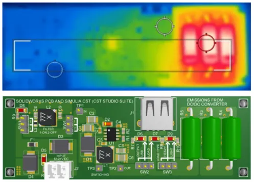
- Use Simulation Tools: Thermal simulation software can help you predict heat flow and identify the best locations for stacked vias. Tools can estimate temperature rises and thermal resistance, guiding your design decisions.
- Optimize Layer Stackup: Design your PCB stackup to include dedicated thermal layers or ground planes that stacked vias can connect to. For example, place a thick copper plane (2oz or more) near the bottom layer to act as a heat spreader.
- Consider Manufacturing Constraints: Stacked vias, especially microvias, can increase manufacturing complexity and cost. Ensure your design adheres to your fabrication partner’s capabilities, such as minimum via size and aspect ratio limits.
- Test and Validate: After prototyping, use thermal imaging or temperature sensors to validate the effectiveness of your stacked vias. Compare actual temperature rises against your simulations to fine-tune future designs.
Conclusion: Making the Right Choice for PCB Heat Dissipation
Effective thermal management is essential for the performance and longevity of electronic devices, and stacked vias offer a powerful solution for heat dissipation in complex PCB designs. They are particularly valuable in high-power, multilayer, or high-density applications where traditional methods like standard thermal vias or heat sinks alone may fall short. By understanding when to use stacked vias—such as in designs with high thermal loads or limited space—and following best practices for their implementation, you can significantly improve your PCB’s thermal performance.
At ALLPCB, we’re committed to helping you achieve optimal results in your PCB projects. Whether you’re tackling thermal challenges or exploring advanced design techniques, our expertise and resources are here to support you. Incorporate stacked vias into your next design to enhance heat dissipation, and experience the difference in reliability and efficiency.


