 ALLPCB


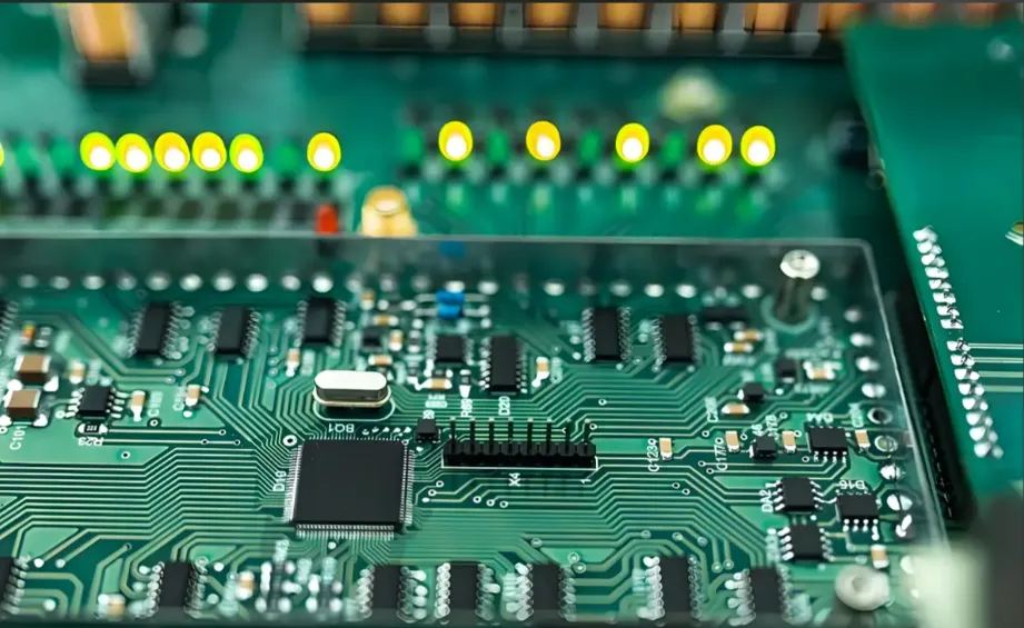
When it comes to mixed technology PCB assembly, combining Surface Mount Technology (SMT) and Through-Hole components, selecting the right panel size is critical for efficiency, cost-effectiveness, and quality. The ideal panel size for mixed technology PCBs depends on factors like component height, assembly processes such as wave soldering, manual insertion requirements, and lead-free soldering challenges. In this comprehensive guide, we'll dive into the key considerations for determining the optimal panel size for SMT and Through-Hole designs, ensuring your project runs smoothly from design to production.
Why Panel Size Matters in Mixed Technology PCB Assembly
Mixed technology PCB assembly involves mounting both SMT and Through-Hole components on the same board, often requiring multiple assembly processes. Panel size—the dimensions of the array of individual PCBs grouped together for manufacturing—directly impacts production efficiency, material usage, and compatibility with assembly equipment. A poorly chosen panel size can lead to increased costs, assembly errors, or delays. Let’s explore how to make informed decisions by addressing key factors like SMT through-hole panel size, wave soldering panel considerations, and more.
Key Factors in Choosing SMT Through-Hole Panel Size
Determining the right panel size for mixed technology PCBs requires balancing several technical and practical considerations. Below, we break down the most important factors to guide your decision-making process.
1. Component Height and Panel Limits
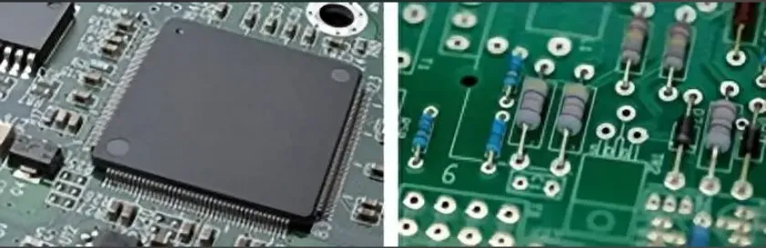
One of the primary challenges in mixed technology PCB assembly is managing component height panel limits. Through-Hole components, such as connectors or capacitors, often have taller profiles compared to SMT parts. During wave soldering, tall components can create shadowing effects, where solder fails to reach certain areas due to obstruction. To avoid this, panel size must allow for adequate spacing between components and ensure compatibility with soldering equipment.
For instance, if Through-Hole components exceed a height of 25 mm, standard wave soldering equipment may struggle to maintain uniform solder flow across the panel. As a general rule, keep panel dimensions within 250 mm x 350 mm for designs with tall components to minimize risks during soldering. Larger panels may require specialized fixtures or multiple passes, increasing production time and cost.
2. Wave Soldering Panel Considerations
Wave soldering is a common method for attaching Through-Hole components in mixed technology PCB assembly. However, wave soldering panel considerations are crucial for achieving consistent results. Panel size directly affects how the board interacts with the solder wave. If the panel is too large—say, exceeding 400 mm in width—it may not fit within standard wave soldering machines, leading to uneven heating or solder defects.
Additionally, larger panels can experience thermal stress during the soldering process, causing warping or misalignment. To mitigate this, consider limiting panel size to 300 mm x 400 mm for most standard equipment. Also, ensure that fiducial marks and tooling holes are placed strategically on the panel to aid in precise alignment during soldering. Proper spacing between individual boards within the panel (typically 5-10 mm) helps prevent solder bridging and allows for easier depanelization after assembly.
3. Panel Size for Manual Insertion
In mixed technology PCB assembly, Through-Hole components often require manual insertion before soldering, especially for low-volume production or prototypes. Choosing the right panel size for manual insertion is essential to streamline this labor-intensive process. Smaller panels, such as those under 200 mm x 250 mm, are generally easier to handle manually, reducing the risk of operator fatigue and insertion errors.
For larger production runs with automated insertion equipment, panel sizes can be slightly larger, up to 350 mm x 450 mm, depending on the machine’s specifications. However, always verify the equipment’s maximum panel size limits to avoid compatibility issues. Additionally, ensure that breakaway tabs or scoring lines between individual boards are designed for easy separation without damaging components near the edges.
4. Lead-Free Soldering Panel Challenges
Lead-free soldering, mandated by regulations like RoHS, introduces unique challenges when selecting panel sizes for mixed technology PCBs. Lead-free solder requires higher melting temperatures (typically 30-40°C hotter than traditional lead-based solder), which can increase thermal stress on the board. Larger panels are more prone to warping under these conditions due to uneven heat distribution.
To address lead-free soldering panel challenges, opt for smaller panel sizes, ideally under 300 mm x 400 mm, to minimize thermal gradients across the board. Additionally, use high-quality PCB materials with better thermal stability, such as FR-4 with a Tg (glass transition temperature) of 170°C or higher. Proper preheat settings during wave soldering can also help reduce thermal shock, especially for larger panels.
Balancing SMT and Through-Hole Requirements in Panel Design
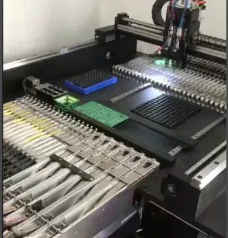
Mixed technology PCB assembly requires careful coordination between SMT and Through-Hole processes, as each has distinct needs that impact panel size. SMT components are typically placed and soldered using reflow ovens before Through-Hole components are inserted and wave soldered. This sequential process means that panel size must accommodate both automated SMT placement machines and wave soldering equipment.
For SMT assembly, panel sizes up to 400 mm x 500 mm are often acceptable, as modern pick-and-place machines can handle larger arrays with high precision. However, when Through-Hole components are added, the panel size may need to be reduced to ensure compatibility with wave soldering constraints, as discussed earlier. A practical compromise is to aim for a panel size of 250 mm x 350 mm, which works well for most mixed technology designs and standard assembly equipment.
Optimizing Panel Size for Cost and Efficiency
Beyond technical considerations, panel size also affects manufacturing costs and production efficiency. Larger panels can reduce material waste and lower per-unit costs by fitting more individual PCBs into a single array. For example, a panel of 300 mm x 400 mm might accommodate 12 individual boards of 70 mm x 80 mm, whereas a smaller 200 mm x 250 mm panel might only fit 6, increasing material and processing costs per board.
However, larger panels come with trade-offs. They may require more complex fixturing, longer soldering times, and additional quality checks to ensure consistency across the entire array. For mixed technology PCB assembly, it’s often more cost-effective to start with a moderate panel size (around 250 mm x 350 mm) and adjust based on specific project needs and equipment capabilities.
Design Tips for Mixed Technology PCB Panels
To ensure your panel size works seamlessly with both SMT and Through-Hole assembly processes, consider the following design tips:
- Standardize Panel Dimensions: Stick to industry-standard panel sizes (e.g., 250 mm x 350 mm or 300 mm x 400 mm) to ensure compatibility with most manufacturing equipment.
- Plan Component Layout: Group Through-Hole components together on one side of the board to simplify wave soldering, and avoid placing tall components near panel edges to prevent damage during depanelization.
- Use Fiducials and Tooling Holes: Include at least three fiducial marks per panel for precise alignment during SMT placement and wave soldering. Tooling holes (typically 3.2 mm in diameter) should be placed in non-critical areas to secure the panel during assembly.
- Account for Depanelization: Design breakaway tabs or V-grooves with a minimum width of 5 mm between individual boards to facilitate easy separation without stressing components.
Common Challenges and How to Overcome Them
Designing and assembling mixed technology PCBs often comes with hurdles related to panel size. Here are some common issues and solutions:
- Thermal Warping: Larger panels are prone to warping during lead-free soldering. Use smaller panels or incorporate stiffeners to maintain flatness.
- Equipment Compatibility: Ensure your panel size matches the specifications of both SMT and wave soldering machines. Consult with your manufacturing partner early in the design phase to confirm limits.
- Component Shadowing: Tall Through-Hole components can block solder flow during wave soldering. Adjust panel size and component placement to minimize shadowing, or consider selective soldering for complex designs.
Conclusion: Making the Right Choice for Your Mixed Technology PCB Panel
Choosing the right panel size for mixed technology PCBs combining SMT and Through-Hole components is a balancing act. Factors like component height panel limits, wave soldering panel considerations, panel size for manual insertion, and lead-free soldering panel challenges all play a role in determining the optimal dimensions. By starting with a moderate panel size—such as 250 mm x 350 mm—and adjusting based on your specific design and equipment needs, you can achieve efficient, high-quality assembly while minimizing costs and risks.
At ALLPCB, we’re committed to helping you navigate the complexities of mixed technology PCB assembly. Whether you’re dealing with SMT through-hole panel size constraints or other design challenges, our expertise and advanced manufacturing capabilities ensure your project succeeds from concept to completion. Take the time to evaluate your panel size carefully, and partner with a trusted provider to bring your vision to life.


