 ALLPCB


In high-speed digital PCB design, controlling trace impedance is critical for maintaining signal integrity. Two key factors that directly impact this are the outer layer copper thickness and the trace geometry. By carefully managing these elements, engineers can ensure reliable performance in applications where data rates exceed 10 Gbps or clock speeds reach into the GHz range. This blog dives deep into the relationship between copper thickness, trace impedance, and signal integrity, offering practical tips and design rules for achieving precise control in high-speed digital designs.
Why Trace Impedance Control Matters in High-Speed Digital PCBs
Trace impedance control is a cornerstone of high-speed digital PCB design. Impedance mismatches can lead to signal reflections, crosstalk, and data errors, especially in circuits handling high-frequency signals. For instance, in a design operating at 5 GHz, even a small mismatch can cause significant signal degradation, impacting the overall system reliability.
In high-speed digital PCBs, signals travel as electromagnetic waves along traces, and the impedance of these traces must match the source and load to minimize reflections. The outer layer copper thickness plays a pivotal role here, as it influences the trace’s cross-sectional area and, consequently, its impedance. Understanding and controlling this relationship is essential for ensuring signal integrity across the board.
What Is Trace Impedance and Why Does It Matter?
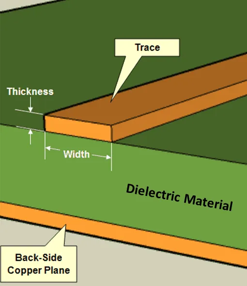
Trace impedance is the measure of opposition to the flow of alternating current in a PCB trace, determined by factors like trace width, height above the ground plane, dielectric material, and copper thickness. For high-speed digital designs, common impedance values are 50 ohms for single-ended signals and 100 ohms for differential pairs. Deviations from these targets can cause signal distortions, leading to bit errors or system failures.
Signal integrity, the quality of the transmitted signal, hinges on maintaining consistent impedance. Poor control can result in issues like overshoot, undershoot, and ringing, which are particularly problematic in applications like DDR4 memory interfaces or USB 3.0 data lines. By focusing on trace impedance control, designers can mitigate these risks and ensure robust performance.
The Role of Outer Layer Copper Thickness in Impedance Control
Copper thickness on the outer layers of a PCB directly affects trace impedance. Thicker copper reduces the resistance of the trace, but it also alters the impedance by changing the trace’s height and effective cross-sectional area. For high-speed digital designs, this relationship must be carefully balanced to meet specific impedance targets.
How Copper Thickness Impacts Impedance
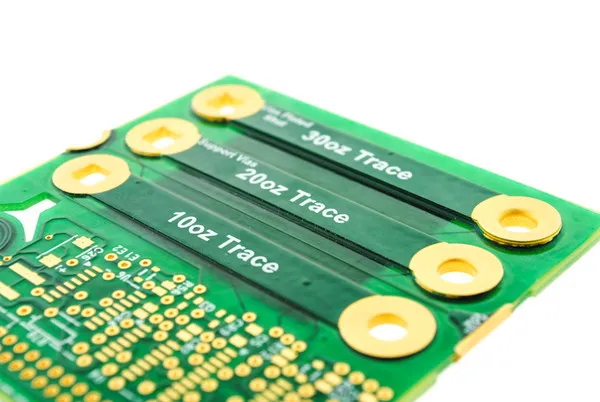
In PCB manufacturing, copper thickness is typically measured in ounces per square foot (oz/ft2), where 1 oz/ft2 equates to approximately 1.4 mils (35 micrometers) of thickness. Common thicknesses for outer layers range from 0.5 oz to 2 oz, depending on the design requirements. Thicker copper, such as 2 oz, is often used for power traces to handle higher currents, while thinner copper, like 0.5 oz, is preferred for high-speed signal traces to achieve finer control over impedance.
The thicker the copper, the lower the trace impedance for a given width, because the increased height changes the electromagnetic field distribution around the trace. For example, a trace with a width of 5 mils on a 1 oz copper layer might have an impedance of 50 ohms, but switching to a 2 oz layer could drop the impedance to 48 ohms if other factors remain constant. This shift might seem small, but in high-speed designs, even a 2-ohm mismatch can degrade signal integrity.
Balancing Copper Thickness with Manufacturing Constraints
While thicker copper can be beneficial for power distribution, it poses challenges for high-speed signal traces. Thicker layers make it harder to achieve narrow trace widths due to etching limitations during manufacturing. For instance, a 2 oz copper layer might require a minimum trace width of 6 mils, whereas a 1 oz layer can support widths as narrow as 3 mils, offering greater flexibility for impedance matching.
Designers must work within these constraints, selecting a copper thickness that balances signal integrity needs with manufacturability. A common practice is to use 1 oz copper for outer layers in high-speed designs, as it provides a good compromise between impedance control and ease of fabrication.
Key PCB Design Rules for Trace Impedance Control
Achieving precise trace impedance control in high-speed digital PCBs requires adherence to specific design rules. These guidelines help ensure consistent impedance across the board, minimizing signal integrity issues. Below are some critical rules to follow:
1. Define Trace Width and Spacing Based on Impedance Targets
Trace width is a primary determinant of impedance. For a 50-ohm single-ended trace on a standard FR-4 substrate with a dielectric height of 5 mils and 1 oz copper, a trace width of approximately 9 mils is often required. However, this value changes with copper thickness and dielectric properties, so designers must use impedance calculators or simulation tools to determine the exact dimensions.
For differential pairs, spacing between the traces also affects impedance. A typical 100-ohm differential pair might require 5-mil wide traces spaced 8 mils apart. Maintaining consistent spacing and symmetry is crucial to avoid common-mode noise and ensure signal integrity.
2. Maintain a Uniform Dielectric Height
The distance between the trace and the reference plane (ground or power) significantly impacts impedance. A thinner dielectric height lowers impedance, while a thicker height increases it. For high-speed designs, a dielectric height of 4-6 mils is common for outer layer traces to achieve standard impedance values. Designers must specify this height in the stack-up and ensure uniformity across the board.
3. Account for Copper Thickness Variations
During manufacturing, copper thickness can vary slightly due to plating and etching processes. A nominal 1 oz layer might range from 1.2 to 1.6 mils in actual thickness, affecting impedance by up to 5%. To mitigate this, designers should collaborate with their fabrication partner to confirm the final copper thickness after plating and adjust trace widths accordingly.
4. Use Controlled Impedance Materials
The dielectric constant (Dk) of the PCB substrate influences impedance. Standard FR-4 has a Dk of around 4.2-4.5, but for high-speed designs, low-loss materials with a Dk of 3.0-3.5 may be preferred to reduce signal attenuation. Specifying the material type and resin content in the stack-up helps achieve consistent impedance.
Signal Integrity Challenges in High-Speed Digital Designs
Signal integrity is the ultimate goal of trace impedance control, but high-speed digital designs face several challenges that can compromise performance. Understanding these issues and their relation to copper thickness and trace design is vital for successful PCB layouts.
Reflections Due to Impedance Mismatches
When a signal encounters a change in impedance along its path, part of the energy reflects back, causing distortion. For example, if a trace transitions from a 50-ohm section to a 55-ohm section due to a change in copper thickness or trace width, reflections can occur, leading to signal ringing. Maintaining uniform impedance through consistent copper thickness and trace geometry prevents this issue.
Crosstalk Between Adjacent Traces
In densely populated high-speed PCBs, traces are often placed close together, increasing the risk of crosstalk. Thicker copper can exacerbate this by strengthening the electromagnetic coupling between traces. To minimize crosstalk, designers should increase spacing between high-speed traces and use ground planes or guard traces as shields.
Signal Attenuation and Loss
High-frequency signals experience greater attenuation in traces with higher resistance, which can occur with thinner copper layers. However, thicker copper increases skin effect losses at high frequencies, where current flows primarily on the surface of the conductor. For designs operating above 5 GHz, a moderate copper thickness of 1 oz often provides the best balance between resistance and skin effect losses.
Practical Tips for Achieving Precise Impedance Control
To help engineers achieve precise trace impedance control in high-speed digital PCBs, here are some actionable tips:
- Use Simulation Tools: Leverage PCB design software with built-in impedance calculators to predict and adjust trace dimensions based on copper thickness and stack-up.
- Collaborate with Fabricators: Work closely with your manufacturing partner to confirm copper thickness, material properties, and achievable trace widths during the design phase.
- Test and Validate: After fabrication, use a Time Domain Reflectometer (TDR) to measure actual impedance and identify any mismatches for future design iterations.
- Standardize Stack-Ups: Develop a consistent stack-up configuration for your high-speed designs to minimize variations in dielectric height and copper thickness across projects.
Conclusion: Mastering Copper Thickness and Impedance for High-Speed Success
In high-speed digital PCB design, outer layer copper thickness and trace impedance are inseparable factors that dictate signal integrity. By understanding how copper thickness influences impedance and adhering to key PCB design rules, engineers can create reliable, high-performing boards for applications with demanding data rates and frequencies. From selecting the right copper thickness to maintaining uniform dielectric heights, every detail matters in achieving precise control.
With careful planning, simulation, and collaboration with fabrication partners, designers can overcome the challenges of impedance control and deliver robust solutions for modern electronics. Whether you're working on a 10 Gbps data link or a GHz-range processor board, mastering these principles ensures your designs meet the highest standards of performance and reliability.
Suggested Image Placement: Add a final image here showing a completed high-speed PCB with highlighted traces and layers. ALT Text: "High-speed digital PCB with optimized traces for signal integrity."


