ALLPCB


When designing a printed circuit board (PCB), one critical decision is whether to use buried vias. But is the investment in buried vias worth it for your project? In short, buried vias can be a valuable choice for complex, high-density designs due to their space-saving and signal integrity benefits, but they come with higher manufacturing costs compared to traditional through-hole vias. The decision hinges on your project’s specific needs, budget, and performance goals.
In this comprehensive guide, we’ll dive deep into the cost analysis of buried vias, compare them with through-hole vias, and explore whether the benefits justify the price. We’ll cover key factors like buried via PCB cost, PCB manufacturing pricing, buried via vs through-hole cost, cost-benefit analysis of buried vias, and PCB design cost optimization. By the end, you’ll have a clear understanding of how to make the best choice for your PCB project.
What Are Buried Vias and Why Do They Matter in PCB Design?
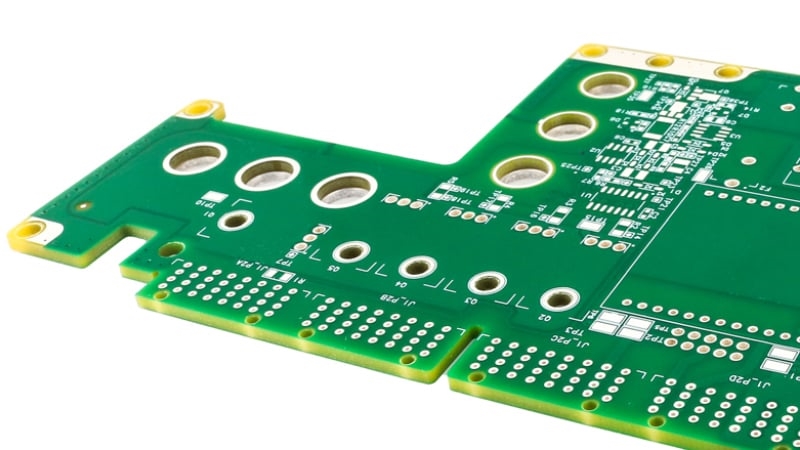
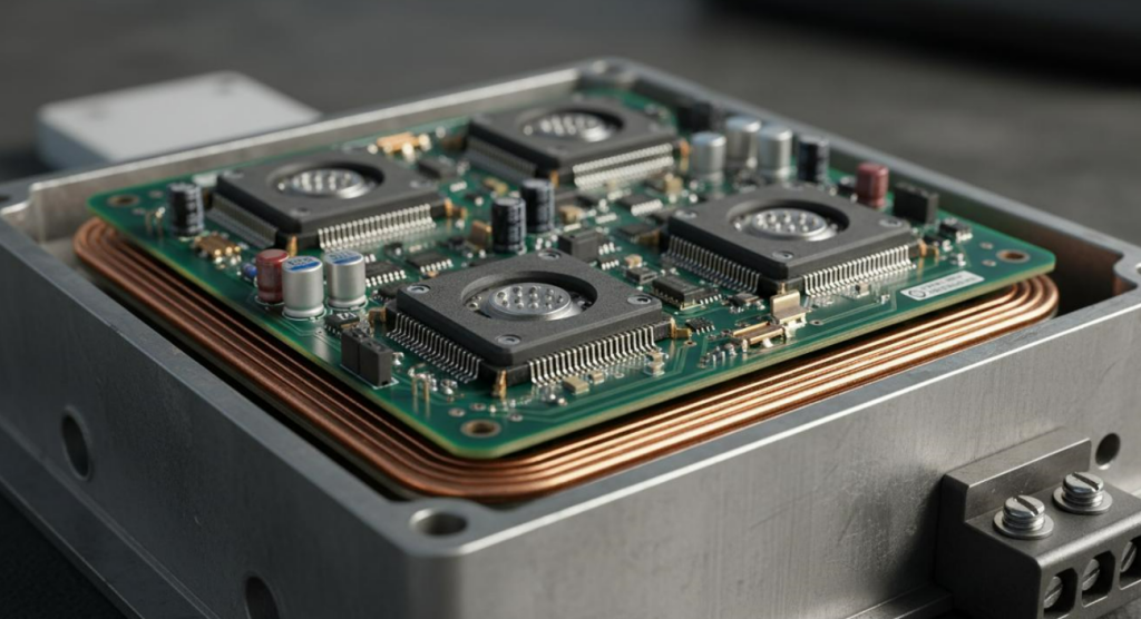
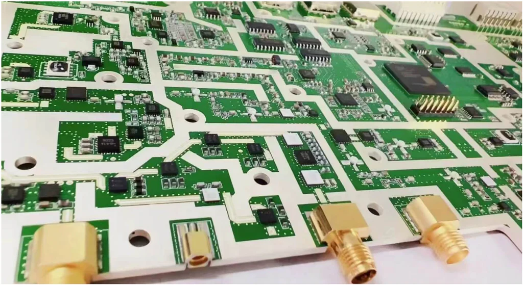
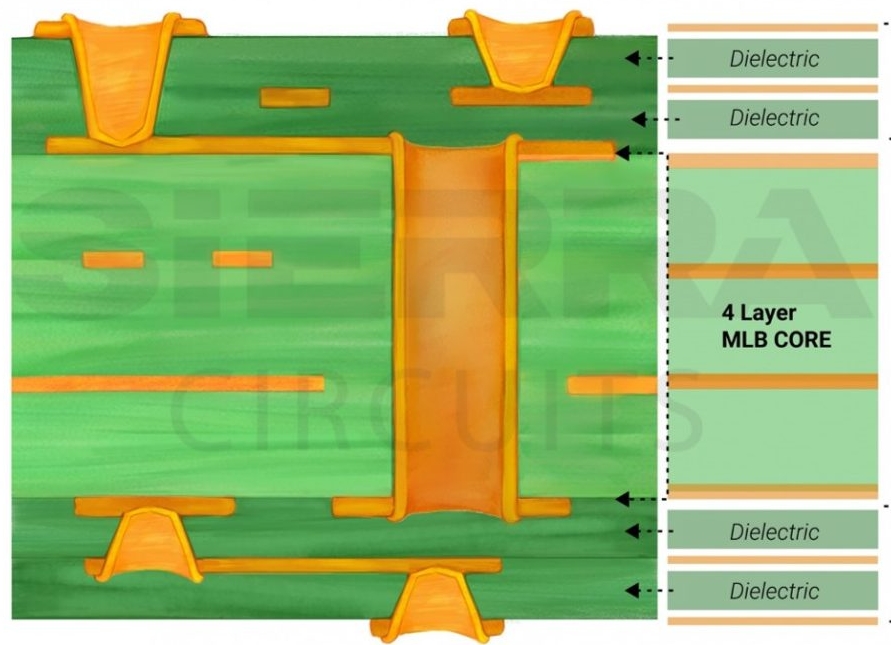
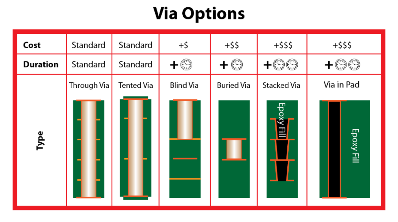
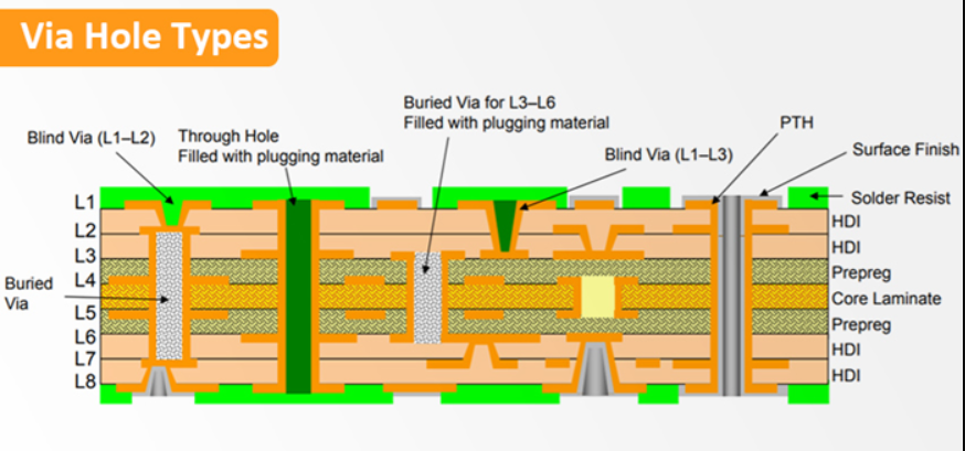
Buried vias are connections between inner layers of a multi-layer PCB that do not extend to the outer surfaces. Unlike through-hole vias, which go through the entire board, or blind vias, which connect an outer layer to an inner one, buried vias are completely hidden within the board’s internal structure. This makes them ideal for high-density interconnect (HDI) designs where space is at a premium.
The primary advantage of buried vias is their ability to free up surface space on the outer layers. This allows for more components or routing on the top and bottom of the PCB. Additionally, buried vias can improve signal integrity by reducing the length of signal paths, which minimizes impedance mismatches and electromagnetic interference (EMI). For high-speed designs, such as those operating at frequencies above 1 GHz, buried vias can help maintain signal speeds and reduce latency.
However, these benefits come at a cost. Let’s break down the financial and technical aspects to see if buried vias are the right fit for your project.
Understanding Buried Via PCB Cost: What Drives the Price?
The cost of implementing buried vias in a PCB design is influenced by several factors. While standard PCB manufacturing pricing varies based on board size, layer count, and materials, buried vias introduce additional expenses due to the complexity of the manufacturing process. Here’s a closer look at the key cost drivers:
- Layer Count and Complexity: Buried vias are typically used in multi-layer boards with 6 or more layers. The more layers, the higher the base cost of the PCB, and buried vias add to this by requiring precise drilling and plating processes between specific layers.
- Manufacturing Process: Creating buried vias involves sequential lamination, where layers are built up step by step. This process is more time-consuming and requires advanced equipment compared to drilling through-hole vias, increasing labor and tooling costs.
- Material Usage: Buried vias often require tighter tolerances and sometimes specialized dielectric materials to maintain signal integrity. These materials can add to the overall expense.
- Volume and Scale: For small batch or prototype runs, the cost per board for buried vias is significantly higher due to setup fees. In larger production runs, the cost per unit decreases, but the upfront investment remains substantial.
While exact pricing depends on the specifics of your design, incorporating buried vias can increase PCB manufacturing costs by 20-50% compared to designs using only through-hole vias. For a complex HDI board with buried vias, costs can range from $2 to $10 per square inch for moderate production volumes, whereas a simpler board without buried vias might cost $1 to $5 per square inch.
Buried Via vs Through-Hole Cost: A Direct Comparison
To fully understand the financial implications, let’s compare buried via vs through-hole cost in detail. Through-hole vias are the traditional choice, drilled straight through all layers of the PCB. They are simpler and cheaper to manufacture but come with limitations in modern, compact designs.
- Manufacturing Cost: Through-hole vias are less expensive because they require a single drilling process through the entire board. Buried vias, on the other hand, demand multiple drilling and lamination steps, driving up costs by as much as 30-40% per via in some cases.
- Design Flexibility: Through-hole vias take up space on all layers, limiting routing options in dense designs. Buried vias free up space, potentially reducing the need for additional layers, which could offset some costs. For example, eliminating just one layer in a 10-layer board can save $0.50 to $1.00 per square inch.
- Performance Impact: In high-frequency applications, through-hole vias can introduce signal delays due to longer paths (e.g., increased impedance of 5-10 ohms over buried vias). Buried vias minimize these issues, potentially reducing the need for costly redesigns or additional components to compensate for signal loss.
In summary, while through-hole vias are more budget-friendly upfront, buried vias may provide long-term savings by optimizing space and performance, especially for compact or high-speed designs.
Cost-Benefit Analysis of Buried Vias: Weighing the Pros and Cons
A thorough cost-benefit analysis of buried vias is essential to determine if they’re worth the investment for your project. Let’s evaluate the advantages and disadvantages from both a technical and financial perspective.
Benefits of Buried Vias
- Space Efficiency: By freeing up surface area, buried vias allow for smaller board sizes or more components. This can reduce overall material costs and enable more compact end products, a critical factor in industries like consumer electronics.
- Improved Signal Integrity: For high-speed designs, buried vias reduce signal path length, lowering impedance and crosstalk. This can improve performance metrics, such as maintaining signal speeds above 5 Gbps with minimal loss.
- Enhanced Reliability: Buried vias are less exposed to external factors like moisture or mechanical stress, potentially increasing the lifespan of the PCB in harsh environments.
Drawbacks of Buried Vias
- Higher Upfront Costs: As discussed, the manufacturing process for buried vias is more complex, leading to increased PCB manufacturing pricing. This can be a barrier for low-budget or prototype projects.
- Design Complexity: Incorporating buried vias requires careful planning and advanced design software, which may increase design time and cost.
- Repair Challenges: Since buried vias are hidden within the board, diagnosing and repairing faults is more difficult and costly compared to through-hole vias.
For projects where performance and compactness are priorities—such as in telecommunications or medical devices—the benefits of buried vias often outweigh the costs. However, for simpler designs or cost-sensitive applications, traditional vias may be the better choice.
PCB Design Cost Optimization: When to Choose Buried Vias
Achieving PCB design cost optimization means balancing performance needs with budget constraints. Here are some scenarios and tips to help you decide if buried vias are the right investment:
- High-Density Designs: If your project requires a high component density, such as in smartphones or IoT devices, buried vias can save space and potentially reduce the number of layers needed, offsetting some of the cost.
- High-Speed Applications: For PCBs handling signals above 1 GHz, buried vias can minimize signal loss and interference, avoiding the expense of additional shielding or redesigns.
- Budget Constraints: If cost is a major concern, consider using a hybrid approach. Combine buried vias only in critical areas of the board with through-hole vias elsewhere to keep expenses down.
- Production Volume: For large-scale production, the per-unit cost of buried vias decreases, making them more viable. For prototypes, stick to simpler via types unless performance testing is critical.
Additionally, work closely with your PCB manufacturer to optimize the design early on. Many offer design-for-manufacturing (DFM) reviews to identify cost-saving opportunities, such as adjusting via placement or layer stack-up to reduce complexity.
Practical Tips for Managing Buried Via PCB Costs
If you decide to incorporate buried vias, there are ways to manage the associated costs effectively:
- Optimize Via Count: Use buried vias only where necessary. Overusing them across the board can unnecessarily inflate costs.
- Standardize Specifications: Stick to standard via sizes and tolerances to avoid custom tooling fees. For instance, using a via diameter of 0.2 mm instead of a non-standard 0.15 mm can save on manufacturing setup costs.
- Plan for Scalability: Design with future production runs in mind. A slightly higher initial investment in buried vias may pay off if it reduces redesign costs for larger batches.
- Collaborate with Manufacturers: Early collaboration can help identify cost-effective alternatives or adjustments to the design that maintain performance while reducing expenses.
Conclusion: Are Buried Vias Worth the Investment?
Deciding whether buried vias are worth the investment for your PCB project comes down to a careful evaluation of your design requirements and budget. While the buried via PCB cost is higher than traditional through-hole vias, the benefits of space savings, improved signal integrity, and enhanced reliability can make them a smart choice for high-density or high-speed applications.
By conducting a thorough cost-benefit analysis of buried vias and focusing on PCB design cost optimization, you can make an informed decision that aligns with your project goals. Whether you’re working on a compact consumer device or a critical industrial system, understanding the trade-offs between buried via vs through-hole cost is key to achieving the best outcome.
Ultimately, buried vias are a powerful tool in modern PCB design, but they’re not a one-size-fits-all solution. Weigh the technical advantages against the increased PCB manufacturing pricing, and choose the approach that delivers the most value for your specific needs.