 ALLPCB


Wireless systems power the modern world, from smartphones and Wi-Fi networks to satellite communications and radar technologies. At the heart of these systems lie RF (Radio Frequency) and Microwave Printed Circuit Boards (PCBs), engineered to handle high-frequency signals with precision and reliability. Designing these specialized PCBs is no simple task—it requires careful attention to detail, advanced materials, and a deep understanding of signal behavior. For engineers, mastering these design considerations can mean the difference between a system that performs flawlessly and one that fails under real-world demands.
In this blog, we'll explore the key factors that shape RF and Microwave PCB design, offering practical insights and actionable advice. Whether you're optimizing signal integrity or managing thermal challenges, these considerations will help you build wireless systems that meet today's high standards. Let's dive into the essentials of creating PCBs that thrive in the fast-paced world of high-frequency electronics.
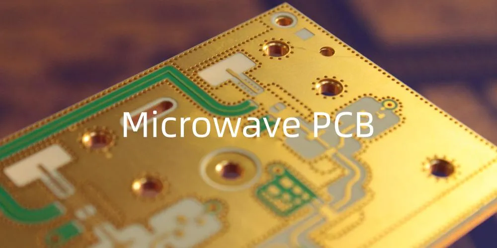
What Makes RF and Microwave PCBs Unique?
RF and Microwave PCBs differ from standard PCBs because they operate at frequencies ranging from 50 MHz to over 300 GHz. RF PCBs typically handle signals up to 1 GHz, while Microwave PCBs cover the higher range, often from 1 GHz to 30 GHz or beyond. These high frequencies introduce unique challenges: signals become more sensitive to noise, impedance mismatches can degrade performance, and even the PCB material itself plays a critical role in signal propagation.
Unlike traditional PCBs, where FR-4 materials suffice for low-frequency applications, RF and Microwave designs demand specialized substrates like PTFE (Teflon), ceramics, or Rogers laminates. These materials offer low dielectric constants (typically 2.2 to 3.5) and low loss tangents (around 0.001 to 0.003), ensuring minimal signal loss and distortion. For engineers, understanding these differences is the first step toward designing a PCB that delivers reliable wireless performance.
Key Design Considerations for RF and Microwave PCBs
To create effective RF and Microwave PCBs, engineers must address several critical factors. Below, we break down the most important considerations and provide practical guidance for tackling them.
1. Material Selection: The Foundation of Performance
The choice of substrate material directly impacts signal integrity and thermal management. Standard FR-4, with a dielectric constant of about 4.5, is affordable but unsuitable for high frequencies due to its high loss tangent (around 0.02) and inconsistent dielectric properties. Instead, we recommend materials like:
- Rogers RO4000 Series: Offers a dielectric constant of 3.38 and a loss tangent of 0.0027, ideal for frequencies above 1 GHz.
- PTFE (Teflon): Provides a low dielectric constant (around 2.1) and excellent thermal stability up to 200°C.
- Ceramic-Filled Laminates: Balances cost and performance with high thermal conductivity.
For multilayer designs, hybrid stack-ups combining high-performance outer layers (e.g., Rogers) with cost-effective inner layers (e.g., FR-4) can optimize both performance and budget. Selecting the right material ensures signals travel at speeds close to 70-80% of the speed of light in a vacuum, minimizing delays in wireless systems.
2. Impedance Matching: Keeping Signals in Check
Impedance matching is non-negotiable in RF and Microwave PCBs. A typical target impedance is 50 ohms, though some applications may require 75 or 100 ohms. Mismatches cause signal reflections, reducing power transfer and introducing noise. To achieve controlled impedance:
- Trace Width and Spacing: Use tools like impedance calculators to determine trace dimensions. For a 50-ohm microstrip on a 1.6 mm Rogers substrate, a trace width of about 0.6 mm is common.
- Ground Planes: Place a continuous ground plane directly beneath RF traces to provide a low-inductance return path.
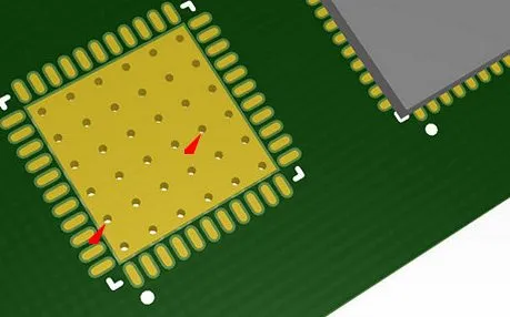
- Via Design: Minimize via use, as they introduce inductance. When necessary, keep aspect ratios low (e.g., 0.8 to 1.2) to reduce signal disruption.
Proper impedance matching can cut signal loss by up to 50%, ensuring efficient power delivery in wireless applications like antennas and transceivers.
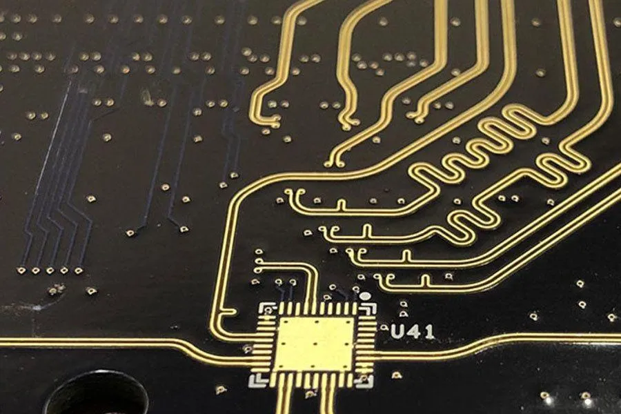
3. Transmission Line Design: Guiding High-Frequency Signals
RF and Microwave PCBs rely on transmission lines—microstrips, striplines, or coplanar waveguides (CPW)—to carry signals. Each type has distinct advantages:
- Microstrips: Simple and cost-effective, placed on the outer layer with a ground plane below. Best for frequencies up to 10 GHz.
- Striplines: Embedded between two ground planes, offering better shielding but requiring multilayer boards. Ideal for 10-30 GHz.
- Coplanar Waveguides: Feature ground planes on the same layer as the signal trace, reducing dispersion and dielectric loss in microwave designs.
Keep traces short and avoid sharp bends—use 45-degree angles or curved paths to maintain signal integrity. For a 5 GHz signal on a Rogers substrate, a microstrip length under 10 mm helps limit attenuation to less than 0.1 dB.
4. Noise Reduction: Protecting Signal Quality
High-frequency signals are highly susceptible to noise, from electromagnetic interference EMI vompliance testing to crosstalk. To minimize these effects:
- Grounding: Use a solid ground plane for each RF layer and connect all grounds with low-impedance vias. This reduces EMI by up to 20 dB.
- Component Placement: Separate RF components from digital or power circuits. For example, place an RF amplifier at least 5 mm away from a microcontroller.
- Decoupling Capacitors: Add 0.1 µF capacitors near power pins to filter noise, cutting power line interference by 30-40%.
Effective noise reduction ensures clear signal transmission, critical for applications like Wi-Fi routers or radar systems.
5. Thermal Management: Handling the Heat
High-frequency components, such as power amplifiers, generate significant heat. Poor PCB thermal management can shift dielectric properties, degrading performance. Solutions include:
- Thermal Vias: Use plated-through vias filled with conductive paste to dissipate heat across layers. A grid of 0.3 mm vias spaced 1 mm apart can reduce hotspot temperatures by 15°C.
- Heat Sinks: Attach heat sinks to high-power components, ensuring a thermal conductivity of at least 50 W/m·K.
- Material Choice: Opt for substrates like aluminum nitride (200 W/m·K) for extreme conditions.
Proper thermal design keeps components within operating limits, extending the lifespan of wireless systems.
6. Stack-Up Design: Balancing Complexity and Performance
A well-planned stack-up enhances routing flexibility and signal isolation. For a 6-layer RF PCB:
- Layer 1: RF traces and components.
- Layer 2: Ground plane.
- Layer 3: Power plane.
- Layer 4-5: Non-RF signals or additional ground.
- Layer 6: Secondary components or routing.
A typical thickness of 1.6 mm provides mechanical stability, but thinner boards (e.g., 0.8 mm) suit compact designs. Align layers precisely during fabrication—misalignment by even 0.1 mm can cause impedance shifts of 5-10 ohms.
7. Shielding: Blocking External Interference
Shielding protects sensitive RF circuits from external EMI. Metal enclosures or shields over RF sections can reduce interference by 30-50 dB. For Microwave PCBs, where wavelengths shrink (e.g., 10 mm at 30 GHz), ensure shield apertures are smaller than one-tenth of the wavelength (1 mm) to prevent leakage.
Overcoming Common Design Challenges
Even with careful planning, RF and Microwave PCB design presents hurdles. Here's how to address two frequent issues:
- Crosstalk: At 5 GHz, a 1 mm spacing between parallel traces cuts crosstalk by 25 dB. Use CPW or striplines for added isolation.
- Skin Effect: At high frequencies, current flows along conductor surfaces, increasing resistance. Gold plating (0.5 µm thick) reduces skin effect loss by 10-15% compared to bare copper.
Simulations using tools like ADS or HFSS can predict these effects, allowing adjustments before fabrication.
How ALLPCB Supports RF and Microwave Design
For engineers tackling RF and Microwave PCB projects, partnering with a reliable manufacturer is key. ALLPCB offers quick-turn prototyping—delivering boards in as little as 24 hours—allowing rapid iteration and testing of high-frequency designs. Our advanced manufacturing capabilities ensure tight tolerances (e.g., ±0.05 mm for trace widths) and support for specialized materials like Rogers and PTFE. With global logistics, we streamline the process from design to delivery, helping you bring wireless systems to market faster and with confidence.
Conclusion: Building the Future of Wireless Systems
Designing RF and Microwave PCBs for wireless systems demands precision, from selecting low-loss materials to mastering impedance and thermal management. By addressing these considerations—material choice, impedance matching, transmission lines, noise reduction, thermal design, stack-up, and shielding—you can create PCBs that power reliable, high-performance wireless technologies. As frequencies climb and applications expand, staying ahead requires both expertise and the right tools.
We hope this guide equips you with the knowledge to tackle your next RF or Microwave project. Have questions or need design support? Feel free to reach out—our team is here to help you succeed in the world of high-frequency electronics.


