ALLPCB


Designing a single-layer PCB with manufacturability in mind is crucial for reducing costs and ensuring a smooth production process. By focusing on Design for Manufacturability (DFM) strategies, you can optimize your single-layer PCB design to minimize errors, lower expenses, and improve overall efficiency. In this comprehensive guide, we’ll explore key DFM techniques tailored for single-layer PCBs, including trace routing optimization, component selection for single-layer boards, and cost reduction strategies through DFM. Whether you're an engineer or a hobbyist, this blog will provide actionable insights to help you achieve a cost-effective and reliable design.
What is DFM and Why Does It Matter for Single-Layer PCBs?
Design for Manufacturability (DFM) refers to the practice of designing products in a way that makes them easy and cost-effective to manufacture. For single-layer PCBs, which are the simplest and often most affordable type of printed circuit boards, applying DFM principles is essential. These boards have conductive traces on only one side, making them ideal for low-complexity circuits, but they also come with unique design challenges.
Implementing DFM strategies in single-layer PCB design helps reduce manufacturing errors, lowers production costs, and speeds up the time to market. With limited space and routing options, every design decision impacts the board's manufacturability. Let’s dive into specific strategies to make your single-layer PCB design both efficient and budget-friendly.

Key DFM Strategies for Single-Layer PCB Design
Below, we break down the most effective DFM strategies for single-layer PCB design, focusing on areas that directly impact cost and manufacturability.
1. Optimize Trace Routing for Simplicity and Efficiency
Trace routing optimization is a cornerstone of DFM for single-layer PCBs. Since you’re limited to one conductive layer, routing must be planned carefully to avoid crossovers and ensure signal integrity while keeping manufacturing costs low.
- Minimize Trace Lengths: Shorter traces reduce material usage and lower the risk of signal degradation. For example, aim to keep high-speed signal traces under 10 inches to maintain signal integrity at frequencies up to 100 MHz.
- Avoid Sharp Angles: Use 45-degree angles instead of 90-degree turns to prevent signal reflection and etching issues during manufacturing. Sharp corners can also lead to acid traps, causing uneven etching.
- Standardize Trace Widths: Stick to common trace widths like 6-8 mils for standard current loads (up to 1A). Wider traces for power lines (e.g., 20-30 mils for 2-3A) ensure proper current handling without overcomplicating the design.
- Maximize Spacing: Maintain at least 6-8 mils of spacing between traces to prevent short circuits and simplify the etching process. This also reduces the chance of manufacturing defects.
By focusing on trace routing optimization, you not only improve the performance of your single-layer PCB but also make it easier and cheaper to produce.

2. Smart Component Selection for Single-Layer Boards
Component selection for single-layer boards plays a significant role in DFM and cost reduction. The right components can simplify assembly, reduce costs, and improve reliability.
- Prioritize Through-Hole Components: Single-layer PCBs often work best with through-hole components because they don’t require vias or additional layers for mounting. These components are also easier to solder manually, reducing assembly costs.
- Use Standard Components: Opt for widely available, standard components over specialized or custom parts. For instance, a common 1kΩ resistor with a 5% tolerance is typically cheaper and easier to source than a precision resistor with a 1% tolerance.
- Minimize Component Count: Reduce the number of unique components to simplify inventory management and lower procurement costs. For example, use a single type of capacitor value across the design if possible.
- Consider Component Placement: Place components on one side of the board to avoid complex assembly processes. Group similar components together to streamline soldering and inspection.
Thoughtful component selection for single-layer boards ensures that your design remains cost-effective while meeting performance requirements.

3. Leverage Cost Reduction Strategies Through DFM
Cost reduction strategies in DFM are all about making smart design choices that align with manufacturing capabilities. For single-layer PCBs, small changes can lead to significant savings.
- Stick to Standard Board Sizes: Use standard panel sizes (e.g., 18x24 inches) to maximize material usage and reduce waste during manufacturing. Custom sizes often increase costs due to inefficient panelization.
- Simplify Drill Holes: Limit the number of drill hole sizes and avoid non-standard diameters. Standard drill sizes (e.g., 0.8mm or 1.0mm) are faster and cheaper to process. Aim for fewer than 5 unique drill sizes per design.
- Choose Cost-Effective Materials: Opt for standard FR-4 material with a thickness of 1.6mm, which is widely used and affordable for single-layer PCBs. Avoid specialty laminates unless absolutely necessary for your application.
- Design for Automated Assembly: If your production involves automated assembly, ensure component spacing and orientation align with pick-and-place machine requirements. This reduces manual labor costs and speeds up production.
Implementing these cost reduction strategies through DFM can cut your manufacturing expenses by up to 10-15%, especially for high-volume production runs.
4. Ensure Proper Design Rules for Manufacturability
Adhering to design rules specific to single-layer PCB DFM is critical for avoiding manufacturing issues. These rules bridge the gap between design intent and production reality.
- Check Minimum Clearances: Ensure a minimum clearance of 6 mils between traces, pads, and board edges to prevent short circuits and manufacturing defects.
- Avoid Overlapping Pads: Overlapping pads can cause soldering issues. Maintain at least 10 mils of separation between adjacent pads.
- Include a Silkscreen Layer: Add a clear silkscreen layer for component labels and orientation markers. This helps during assembly and reduces the risk of errors, saving time and cost.
- Test Points for Debugging: Include accessible test points in your design to simplify quality checks during manufacturing. Place them on the top layer for easy access.
Following these design rules ensures that your single-layer PCB is ready for production without costly revisions.
Common Challenges in Single-Layer PCB DFM and How to Overcome Them
While single-layer PCBs are simpler than multi-layer designs, they come with unique challenges. Here’s how to address them using DFM principles.
1. Limited Routing Space
With only one conductive layer, routing all traces without crossovers can be difficult. To overcome this, plan your component placement first to minimize trace intersections. Use jumpers or zero-ohm resistors as a cost-effective solution for unavoidable crossovers.
2. Signal Integrity Issues
Single-layer PCBs are prone to noise and interference, especially for high-speed signals. Keep sensitive traces away from power lines and maintain a ground plane area if possible, even on a single layer, by dedicating a section of the board to ground.
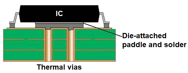
3. Thermal Management
Without additional layers for heat dissipation, thermal management can be a concern. Use wider traces for power components and add thermal vias or copper pours near heat-generating parts to spread heat effectively.
Benefits of Applying DFM to Single-Layer PCB Design
By integrating DFM strategies into your single-layer PCB design process, you gain several advantages:
- Lower Production Costs: Optimized designs reduce material waste, simplify assembly, and minimize errors, saving money at every stage.
- Faster Turnaround Times: A manufacturable design means fewer revisions and quicker production cycles, getting your product to market faster.
- Improved Reliability: DFM ensures that your design accounts for real-world manufacturing constraints, leading to more reliable boards.
Final Tips for Cost-Effective Single-Layer PCB Design
Before finalizing your single-layer PCB design, consider these additional tips to maximize cost savings and manufacturability:
- Always review your design with manufacturing guidelines in mind. Many PCB design tools include DFM checks to flag potential issues before production.
- Collaborate with your manufacturer early in the design process to understand their specific capabilities and limitations.
- Start with a prototype run to test your design in small quantities before committing to large-scale production.
Conclusion
Designing a single-layer PCB with DFM strategies in mind is a powerful way to achieve cost-effective and reliable results. By focusing on trace routing optimization, smart component selection for single-layer boards, and cost reduction strategies through DFM, you can streamline the manufacturing process and save on production expenses. Whether you’re working on a simple hobby project or a commercial product, applying these single-layer PCB DFM techniques ensures that your design is both practical and budget-friendly.
With careful planning and attention to detail, your single-layer PCB can meet performance goals without breaking the bank. Use the insights from this guide to refine your design process and create boards that are easy to manufacture and cost-efficient to produce.