 ALLPCB


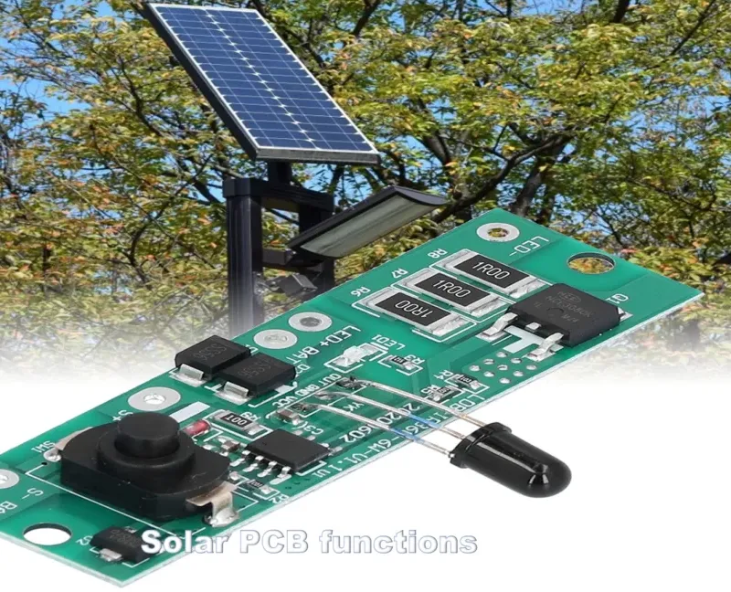
In the rapidly growing field of renewable energy, solar technology stands out as a key player, and the heart of any solar system lies in its printed circuit boards (PCBs). If you're searching for a comprehensive resource on solar PCB SMT assembly, through hole solar PCB components, or soldering techniques like reflow soldering solar PCB and wave soldering solar PCB, you've come to the right place. This guide will walk you through the essentials of assembling PCBs for solar applications, covering both Surface Mount Technology (SMT) and Through-Hole Technology (THT), along with practical tips for using solder paste solar PCB applications. Let's dive into the details to help you achieve reliable, high-performance solar PCBs.
Why Solar PCB Assembly Matters
Solar PCBs are the backbone of solar energy systems, controlling everything from power conversion to energy storage. Whether you're designing a small solar-powered device or a large-scale solar farm controller, the quality of your PCB assembly directly impacts efficiency, durability, and performance. Solar PCBs must withstand harsh environmental conditions like extreme temperatures, humidity, and UV exposure, making precision in assembly techniques critical.
In this guide, we'll explore two primary assembly methods—SMT and THT—and discuss how soldering processes like reflow and wave soldering play a role in creating robust solar PCBs. By understanding these techniques, you can ensure your solar projects meet industry standards and deliver long-term reliability.
Understanding Solar PCB Assembly: SMT vs. Through-Hole
PCB assembly for solar applications typically involves two main techniques: Surface Mount Technology (SMT) and Through-Hole Technology (THT). Each method has its unique advantages, and choosing the right one depends on your project's specific needs, such as size constraints, power requirements, and environmental durability.
What is Solar PCB SMT Assembly?
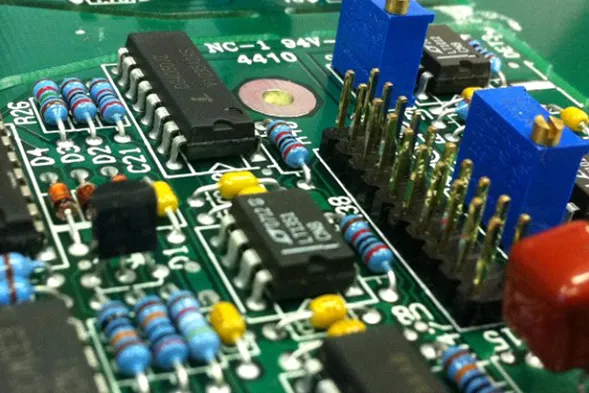
Solar PCB SMT assembly involves mounting components directly onto the surface of the PCB. This method is widely used in modern solar electronics due to its ability to support compact designs and high component density. SMT components are smaller, allowing for more efficient use of board space—a critical factor in solar devices where size and weight often matter.
Key benefits of SMT for solar PCBs include:
- Compact Design: SMT components can be as small as 0.4mm x 0.2mm, enabling high-density layouts ideal for portable solar chargers or compact inverters.
- Cost-Effective Production: Automated SMT assembly reduces labor costs and speeds up manufacturing, with placement machines achieving rates of up to 100,000 components per hour in high-volume settings.
- Improved Performance: Shorter connection paths in SMT designs reduce signal loss and electromagnetic interference, enhancing the efficiency of solar power management circuits.
However, SMT components can be less durable under mechanical stress, which may be a concern for solar installations in rugged environments. Proper design and soldering techniques are essential to ensure reliability.
What are Through-Hole Solar PCB Components?
Through hole solar PCB components are mounted by inserting their leads through holes drilled in the PCB and soldering them on the opposite side. This traditional method is still relevant for solar applications, especially for components that require high mechanical strength or handle significant power loads, such as connectors, relays, and large capacitors in solar inverters.
Advantages of THT for solar PCBs include:
- Durability: Through-hole components are more resistant to vibration and thermal stress, making them suitable for solar systems exposed to harsh outdoor conditions.
- High Power Handling: THT is often used for components that manage high currents (e.g., 10A or more), which are common in solar battery management systems.
- Easier Repairs: Components with leads are simpler to replace manually, which can be a benefit for field maintenance of solar equipment.
The trade-off is that THT takes up more space and is slower to assemble, often requiring manual soldering or additional processing steps compared to SMT.
Soldering Techniques for Solar PCB Assembly
Soldering is a critical step in PCB assembly, ensuring that components are securely connected to the board both electrically and mechanically. For solar PCBs, where reliability under varying conditions is paramount, choosing the right soldering method and materials is essential. Let's explore the key techniques and considerations, focusing on solder paste solar PCB applications, reflow soldering solar PCB, and wave soldering solar PCB.
Solder Paste in Solar PCB Assembly
Solder paste solar PCB applications are a cornerstone of SMT assembly. Solder paste, a mixture of tiny solder particles and flux, is applied to the PCB using a stencil before components are placed. When heated, the paste melts to form strong electrical connections. For solar PCBs, selecting the right solder paste is crucial to ensure long-term reliability under temperature cycling (e.g., -40°C to 85°C in outdoor solar applications).
Key considerations for solder paste in solar PCB assembly:
- Lead-Free Options: Many solar projects adhere to environmental regulations like RoHS, requiring lead-free solder paste with melting points around 217°C to 221°C.
- Flux Type: No-clean flux is often preferred for solar PCBs to avoid residue that could corrode under humid conditions.
- Application Precision: Stencil thickness (typically 0.1mm to 0.15mm) must be optimized to prevent solder bridging or insufficient paste, which can lead to weak joints.
Proper storage of solder paste at 2°C to 10°C and thorough mixing before use are also vital to maintain its performance during solar PCB assembly.
Reflow Soldering for Solar PCB
Reflow soldering solar PCB is the primary method used in SMT assembly. After applying solder paste and placing components, the PCB passes through a reflow oven where controlled heating melts the paste, forming solid solder joints. This process is ideal for high-volume solar PCB production due to its automation and consistency.
Steps in the reflow soldering process for solar PCBs:
- Preheat Zone: Gradually raises the PCB temperature to 150°C to 180°C over 60-90 seconds to activate flux and prevent thermal shock.
- Soak Zone: Maintains a steady temperature (around 180°C to 200°C) for 60-120 seconds to ensure even heating across the board.
- Reflow Zone: Peaks at 230°C to 250°C for 20-40 seconds, melting the solder paste to form joints.
- Cooling Zone: Slowly cools the PCB to solidify solder joints without creating internal stresses.
For solar PCBs, reflow profiles must be tailored to prevent overheating sensitive components like microcontrollers or sensors, which are common in solar tracking or monitoring systems. Using nitrogen atmospheres during reflow can also reduce oxidation, improving joint quality for outdoor reliability.
Wave Soldering for Solar PCB
Wave soldering solar PCB is typically used for through-hole components. In this process, the PCB passes over a wave of molten solder, which adheres to the exposed metal areas, creating strong connections. Wave soldering is efficient for assembling solar PCBs with a mix of THT components, such as power connectors or large diodes in solar charge controllers.
Key aspects of wave soldering for solar PCBs:
- Temperature Control: Solder bath temperatures are maintained at 250°C to 260°C to ensure proper wetting without damaging components.
- Flux Application: A flux layer is applied before soldering to clean surfaces and improve solder adhesion, critical for reliable connections in high-humidity solar environments.
- Conveyor Speed: Speeds of 1.0 to 1.5 meters per minute are typical to balance throughput and solder quality.
While wave soldering is less common in fully SMT designs, it remains a valuable technique for hybrid solar PCBs that combine SMT and THT components. Careful masking of SMT areas is necessary to prevent solder from affecting surface-mounted parts during the wave process.
Best Practices for Solar PCB Assembly
To ensure the success of your solar PCB assembly, whether using SMT or THT techniques, follow these best practices tailored for solar applications:
- Material Selection: Choose PCB substrates like FR-4 with high thermal resistance (Tg of 150°C or higher) to withstand solar operating conditions.
- Component Placement: For SMT, use automated pick-and-place machines with accuracy down to 0.01mm for precision. For THT, ensure proper lead alignment to avoid stress on solder joints.
- Thermal Management: Incorporate heat sinks or thermal vias in solar PCB designs to dissipate heat from power components, preventing failures at temperatures above 85°C.
- Environmental Testing: Subject assembled solar PCBs to thermal cycling (-40°C to 85°C) and humidity tests (85% RH) to simulate real-world conditions.
- Quality Control: Use Automated Optical Inspection (AOI) systems post-soldering to detect defects like solder bridges or misaligned components at a resolution of 5 microns or better.
By adhering to these practices, you can enhance the reliability and lifespan of solar PCBs, ensuring they perform optimally in demanding environments.
Challenges in Solar PCB Assembly and How to Overcome Them
Assembling PCBs for solar applications comes with unique challenges due to the need for durability and efficiency. Here are common issues and solutions:
- Thermal Stress: Solar PCBs face wide temperature swings. Use components rated for extended temperature ranges and apply conformal coatings to protect against thermal expansion mismatches.
- Moisture and Corrosion: Outdoor solar systems are exposed to humidity. Opt for no-clean flux and apply protective coatings with dielectric strengths of 50kV/mm or higher.
- Power Efficiency: Inefficient soldering can lead to resistance in joints, reducing power output. Ensure precise solder paste application and reflow profiles to achieve joint resistance below 0.1 milliohms.
Conclusion: Building Reliable Solar PCBs with SMT and Through-Hole Techniques
Assembling PCBs for solar applications requires a deep understanding of both solar PCB SMT assembly and through hole solar PCB components, along with mastery of soldering methods like reflow soldering solar PCB and wave soldering solar PCB. By leveraging the compact efficiency of SMT and the robust strength of THT, and by optimizing solder paste solar PCB applications, you can create high-performance boards tailored to the unique demands of solar technology.
Whether you're designing a small solar gadget or a large-scale energy system, the techniques and best practices outlined in this guide will help you achieve reliable, durable results. Focus on precision in assembly, select materials suited for harsh environments, and rigorously test your boards to ensure they meet the challenges of solar applications. With the right approach, your solar PCBs will power the future of clean energy with efficiency and longevity.


