 ALLPCB


Designing high-layer-count PCBs for automated assembly is a critical skill for engineers looking to streamline production and ensure reliability. Whether you're working on complex electronics for telecommunications, aerospace, or consumer devices, optimizing your PCB design for assembly can save time, reduce costs, and improve performance. In this comprehensive guide, we'll explore how to enhance your PCB automated assembly process, focus on PCB design for assembly, and integrate SMT PCB techniques for high-layer-count boards. Let’s dive into actionable strategies and best practices to achieve seamless manufacturing.
Why Optimize High-Layer-Count PCB Designs for Automated Assembly?
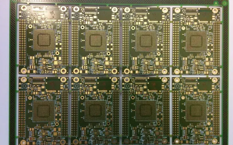
High-layer-count PCBs, often defined as boards with eight or more layers, are essential for modern electronics that demand dense interconnects and high-speed performance. These boards handle complex circuits in limited space, making them ideal for advanced applications. However, their complexity poses challenges during automated assembly, especially with surface mount technology (SMT). Without proper optimization, issues like component misalignment, soldering defects, and signal integrity problems can arise, leading to costly rework or failures.
Optimizing your design ensures compatibility with automated pick-and-place machines, reflow soldering processes, and inspection systems. This results in faster production cycles, lower error rates, and improved product quality. By focusing on PCB design for assembly, you can minimize manual intervention and maximize efficiency in PCB automated assembly.
Key Challenges in High-Layer-Count PCB Assembly
Before diving into optimization strategies, it's important to understand the unique challenges of assembling high-layer-count PCBs:
- Component Density: With multiple layers, components are often packed tightly, increasing the risk of placement errors during SMT PCB assembly.
- Thermal Management: High-layer boards generate more heat, which can affect soldering quality and component reliability if not addressed in the design phase.
- Signal Integrity: More layers mean more potential for crosstalk and impedance mismatches, requiring precise trace routing and layer stacking.
- Manufacturing Tolerances: Automated assembly equipment demands strict adherence to design tolerances to avoid misalignments or defects.
Addressing these challenges through design optimization is the foundation of successful PCB automated assembly.
Best Practices for Optimizing PCB Design for Automated Assembly
Let’s explore practical steps to optimize high-layer-count PCB designs for automated assembly. These strategies focus on compatibility with SMT PCB processes and aim to reduce errors during production.
1. Plan Your Layer Stack-Up for Manufacturability
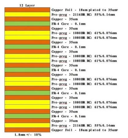
The layer stack-up defines how layers are arranged in your PCB, impacting both signal integrity and assembly. For high-layer-count boards, a balanced stack-up is crucial to prevent warping during manufacturing. Aim for symmetry by placing signal and ground planes in a way that evenly distributes stress. For instance, a 12-layer PCB might follow a structure like Signal-Ground-Signal-Power-Signal-Ground (repeated for symmetry).
Additionally, ensure that inner layers are accessible for vias and routing without overcrowding. This reduces the risk of drilling errors during fabrication, which can affect automated assembly alignment. Work closely with your manufacturing partner to confirm stack-up feasibility and material choices, such as FR-4 or high-Tg laminates for thermal stability.
2. Optimize Component Placement for SMT Compatibility
Component placement directly impacts the efficiency of PCB automated assembly. Automated pick-and-place machines require clear access to component pads, so avoid placing parts too close together. Maintain a minimum spacing of 0.5 mm between components to prevent placement errors, especially for fine-pitch devices like QFNs or BGAs commonly used in high-layer designs.
Group similar components together to minimize machine head movement during assembly. For example, place all 0402 resistors in one area to allow the machine to pick and place them in a single pass. Also, orient components in the same direction to simplify programming for assembly equipment. This reduces setup time and enhances accuracy in SMT PCB processes.
3. Design for Thermal Balance During Reflow Soldering
High-layer-count PCBs often have uneven copper distribution across layers, leading to thermal imbalances during reflow soldering. Excessive heat in one area can cause tombstoning (components lifting on one side) or poor solder joints. To mitigate this, balance copper density by adding dummy fills or ground pours in areas with low copper content.
Pay attention to thermal pads under components like power ICs. Ensure these pads have sufficient vias (e.g., 9-16 vias under a 5x5 mm pad) to dissipate heat across layers. This prevents overheating during soldering and ensures reliable connections in PCB automated assembly.
4. Minimize Via Complexity for Assembly and Signal Integrity
Vias are critical in high-layer-count PCBs for connecting traces across layers, but excessive or poorly designed vias can complicate assembly and degrade signal performance. Use microvias (diameter < 0.15 mm) for high-density interconnects, as they save space and support finer pitch components. However, limit via-in-pad designs unless necessary, as they can trap solder paste during SMT PCB assembly, causing defects.
For high-speed signals, maintain controlled impedance by matching via lengths and avoiding stubs. A typical target impedance for high-speed traces is 50 ohms, which requires careful calculation of via dimensions and layer transitions. Tools like impedance calculators can help achieve this precision in your PCB design for assembly.
5. Ensure Clear Silkscreen and Fiducial Marks for Automation
Automated assembly relies on vision systems to align components accurately. Fiducial marks—small copper dots on the PCB surface—act as reference points for these systems. Place at least three fiducial marks on opposite corners of the board, with a diameter of 1-2 mm and a clear zone (no components or traces) of 3 mm around each mark.
Similarly, ensure silkscreen labels are legible and positioned away from pads or vias. This helps operators and machines identify components or test points without confusion, streamlining the PCB automated assembly process.
6. Adhere to Design for Manufacturability (DFM) Guidelines
DFM guidelines bridge the gap between design and manufacturing, ensuring your PCB is assembly-ready. For high-layer-count boards, key DFM rules include:
- Minimum Trace Width/Spacing: Use at least 0.1 mm (4 mils) for traces and spacing to avoid fabrication issues.
- Pad Sizes: Match pad sizes to component footprints, ensuring they are 0.2-0.3 mm larger than the component lead for soldering reliability.
- Solder Mask Clearance: Maintain a 0.05 mm clearance around pads to prevent mask overlap during SMT PCB assembly.
Running a DFM check before finalizing your design can catch potential issues early, saving time and cost in production.
Advanced Tips for SMT PCB Assembly in High-Layer Designs
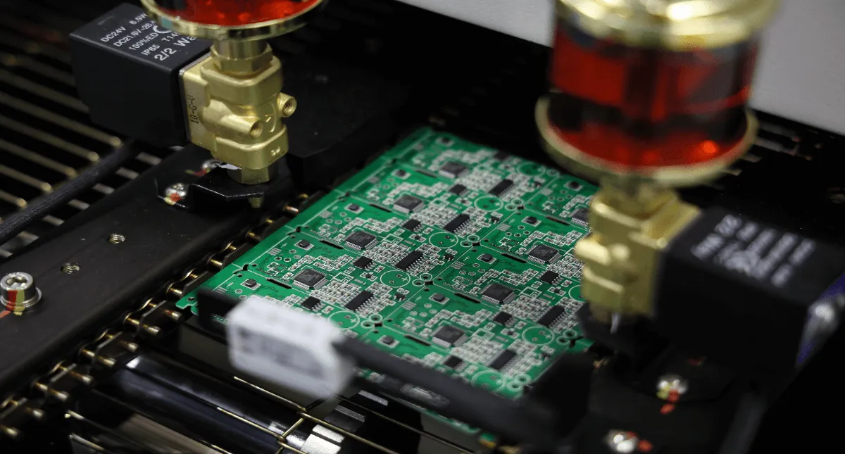
Surface mount technology is the backbone of modern PCB automated assembly, especially for high-layer-count boards. Here are advanced tips to refine your SMT PCB design:
- Use Standard Footprints: Stick to industry-standard footprints for components to ensure compatibility with assembly libraries and reduce programming errors.
- Optimize Stencil Design: For fine-pitch components, design solder paste stencils with a thickness of 0.1-0.15 mm and aperture reductions of 10-20% to prevent excess paste and bridging.
- Plan for Inspection: Leave space for automated optical inspection (AOI) by avoiding tall components near test points. This ensures defects like misaligned parts are caught early.
Signal Integrity and Testing Considerations
High-layer-count PCBs often support high-speed signals, where even small design flaws can cause failures. Maintain signal integrity by routing critical traces on inner layers shielded by ground planes. Keep trace lengths short for differential pairs, targeting a length mismatch of less than 5 mm to avoid timing issues at speeds above 1 GHz.
After assembly, testing is vital to validate performance. Incorporate test pads for in-circuit testing (ICT) on critical nets, spacing them at least 2.54 mm apart for probe access. This ensures your PCB design for assembly supports quality control without redesigns.
Benefits of Optimized PCB Design for Automated Assembly
Investing time in optimization yields significant returns during production:
- Reduced Costs: Fewer assembly errors mean less rework, saving up to 30% on production expenses.
- Faster Turnaround: Streamlined designs can cut assembly time by 20-40%, accelerating time-to-market.
- Higher Reliability: Proper thermal and signal management reduces failure rates, enhancing product lifespan.
By focusing on PCB automated assembly compatibility, you create boards that perform better and cost less to produce.
Conclusion: Mastering High-Layer-Count PCB Design for Assembly
Optimizing high-layer-count PCB designs for automated assembly is a blend of strategic planning and attention to detail. From layer stack-up to component placement, every design decision impacts the efficiency of PCB automated assembly and the quality of the final product. By following best practices like DFM adherence, thermal balancing, and signal integrity management, you can overcome the challenges of complex boards and achieve seamless SMT PCB production.
Start integrating these tips into your PCB design for assembly workflow to enhance manufacturability and performance. With the right approach, even the most intricate high-layer-count PCBs can be assembled with precision and reliability, paving the way for cutting-edge electronics.


