ALLPCB


Introduction
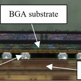
Ball grid array (BGA) packages have become essential in modern electronics due to their high pin counts and compact footprints. These components feature solder balls arranged in a grid under the package, connecting to the PCB pads during reflow soldering. However, the hidden nature of these solder joints makes traditional optical inspection impossible, necessitating advanced techniques like BGA solder joint X-ray. This guide explores the principles, practices, and benefits of X-ray inspection for ensuring BGA reliability. Factory engineers rely on ball grid array inspection to detect defects that could compromise performance in demanding applications. Ultimately, X-ray void detection BGA plays a critical role in maintaining quality control standards.
What Is X-Ray Inspection for BGA Packages and Why It Matters
X-ray inspection for BGA packages involves directing X-rays through the assembly to produce images revealing internal structures. Solder, being denser than surrounding materials, appears brighter on these grayscale images, while voids show as darker areas. This non-destructive method allows engineers to evaluate hundreds of hidden joints simultaneously without disassembly. In high-volume manufacturing, ball grid array inspection via X-ray ensures compliance with quality requirements for critical sectors like automotive and aerospace.
The importance stems from the potential for defects to cause field failures. Voids in solder joints reduce mechanical strength and thermal conductivity, leading to cracks under thermal cycling. Bridges can short circuits, while missing or non-wet balls create opens. IPC-7095D emphasizes X-ray as a key tool for BGA assembly verification, highlighting its role in process optimization. Without routine BGA solder joint X-ray, latent defects escape detection, increasing rework costs and reliability risks. Factory-driven insights confirm that consistent X-ray use correlates with higher first-pass yields.
Technical Principles of X-Ray Inspection
X-ray systems generate a beam that penetrates the PCB assembly, with attenuation varying by material density. Thicker or denser regions absorb more radiation, resulting in lighter shades on the detector. For BGA packages, this reveals solder ball shape, size, and continuity from pad to package. Standard 2D transmission views provide an overview but can obscure overlapping features in dense grids.
To overcome limitations, oblique or 2.5D angled views tilt the board or source, separating adjacent balls for clearer void and bridge assessment. Advanced 3D computed tomography (CT) reconstructs volumetric images by rotating the sample, offering precise measurements of defect depth and volume. X-ray void detection BGA excels here, as gas pockets appear distinctly dark against solder. System resolution, typically sub-micron for fine-pitch BGAs, determines small void visibility.
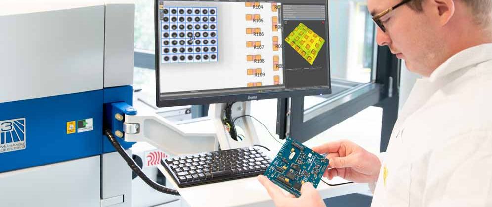
Image contrast and magnification further enhance analysis. Automatic X-ray inspection (AXI) systems use algorithms to quantify defects across the array. Factors like tube voltage and flux affect penetration and clarity.
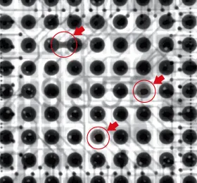
Common Defects Detected by BGA Solder Joint X-Ray
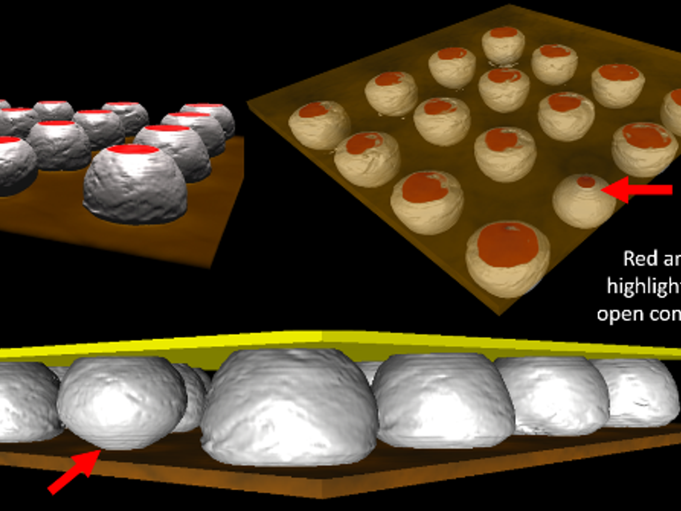
Voids represent one of the most frequent issues, forming from outgassing during reflow or flux entrapment. IPC-7095D classifies voids by size and location, noting center voids impact reliability less than those near interfaces. On X-ray, multiple small voids merge visually, requiring careful measurement protocols.
Solder bridges occur when excess material connects adjacent balls, appearing as fused bright areas. Head-in-pillow defects show a pillow-like package offset from the solder mass, often due to warpage or timing mismatches. Non-wet opens display isolated pads without solder fillet, while missing balls leave empty grid positions.
Cracks and lifted balls manifest as irregular shapes or discontinuities. These defects compromise electrical and thermal paths, accelerating under vibration or temperature swings.
Best Practices for Ball Grid Array Inspection
Establish a standardized X-ray protocol aligned with factory processes. Calibrate systems daily for consistent voltage, current, and geometry to match reference good joints. Use multiple views: top-down for alignment, 45-degree obliques for bridging, and laminographic slices for volume voids.
For X-ray void detection BGA, follow IPC-7095D guidelines on image acquisition and analysis. Measure void percentage by projecting area against ball diameter, accounting for projection distortions. Implement sampling plans, inspecting 100% for high-reliability Class 3 per J-STD-001, or statistical for Class 2.
Integrate AXI for high-throughput, with manual review for anomalies. Train operators on terminology like pixel pitch and grayscale thresholds. Correlate X-ray findings with electrical testing to validate.
Document thresholds: reject if voids exceed process specs, bridging present, or balls misaligned beyond tolerance. Post-inspection, track trends to refine reflow profiles.
Troubleshooting Insights from Factory Experience
In practice, excessive voids often trace to nitrogen reflow atmospheres or stencil aperture designs. Review thermal profiles to ensure peak temperatures promote complete flux volatilization without solder disruption. Warpage mismatches cause head-in-pillow; measure package and PCB bow using shadow moire before assembly.
If X-ray reveals inconsistent ball sizes, inspect incoming BGA components for coplanarity per IPC-7095D. Bridges signal paste volume overload; adjust stencil thickness or printing pressure. For subtle cracks, supplement with acoustic microscopy.
A common pitfall is over-reliance on 2D views, missing stacked voids resolved by 3D CT. Factory data shows 3D reduces false calls by 40%, though throughput trade-offs apply. Iterative process tweaks, guided by X-ray feedback, minimize escapes.
Conclusion
X-ray inspection stands as the cornerstone of BGA quality control, enabling precise ball grid array inspection invisible to other methods. From void detection to bridge identification, it safeguards joint integrity against failure modes. Adhering to standards like IPC-7095D and J-STD-001 ensures consistent, factory-proven outcomes. Engineers benefit from structured protocols that balance thoroughness and efficiency. Implementing these practices elevates assembly reliability, reducing long-term costs. Prioritize BGA solder joint X-ray for robust electronics production.
FAQs
Q1: What is BGA solder joint X-ray inspection?
A1: BGA solder joint X-ray uses radiation to image hidden solder connections under ball grid array packages. It reveals defects like voids, bridges, and misalignments non-destructively. Factory protocols per IPC-7095D specify views and analysis for accurate assessment. This method supports high-volume quality control without disassembly.
Q2: How does X-ray void detection BGA improve reliability?
A2: X-ray void detection BGA identifies gas pockets weakening mechanical and thermal performance. Voids near joint interfaces pose higher risks, as noted in standards. Quantitative measurement guides process corrections, preventing cracks in service. Regular inspection correlates with extended field life in demanding environments.
Q3: What are best practices for ball grid array inspection using X-ray?
A3: Select systems with oblique and 3D capabilities for comprehensive coverage. Calibrate for fine-pitch resolution and use multi-angle imaging to avoid overlaps. Align with J-STD-001 for Class 3 100% checks. Trend analysis from X-ray data refines reflow and stencil parameters effectively.
Q4: When is 3D X-ray preferred over 2D for BGA inspection?
A4: 3D X-ray excels for volumetric void analysis and stacked defect separation in dense BGAs. It provides precise measurements unavailable in 2D projections. Use for high-reliability applications or troubleshooting per IPC-7095D. Trade higher time for superior accuracy in critical joints.
References
IPC-7095D — Design and Assembly Process Implementation for Ball Grid Arrays. IPC.
IPC-A-610 — Acceptability of Electronic Assemblies. IPC.
J-STD-001 — Requirements for Soldered Electrical and Electronic Assemblies. IPC/JEDEC.