ALLPCB


Introduction
Health is a key concern for individuals and society. Wearable medical monitoring systems can conveniently collect health data for disease prediction and early diagnosis. Wearable medical chip solutions based on low-cost, low-power, and high-throughput wireless communication technologies enable continuous collection of basic vital signs during daily activities. By reducing face-to-face consultation time, they can shorten patient waiting times at clinics and help relieve pressure on limited medical resources while improving the quality of care. Chronic diseases such as hypertension, diabetes, and hyperlipidemia require long-term, continuous monitoring of patient data. Wearable medical chips are attractive because of their small size, low power consumption, and low usage cost, encouraging adoption and drawing many semiconductor companies into development and commercialization.
Examples of wearable sensors include fingertip pulse oximeters, wrist-worn glucose sensors, wrist sleep-quality monitors, sleep physiology recorders, belt-type respiration and heartbeat monitors, and implantable identification modules. A wireless wearable microsystem consists of multiple wireless sensors placed on the body surface, integrated into clothing, watches, or jewelry. Physical wires between sensors and a central processing/display chip are inconvenient and can be cumbersome. Wireless communication as a replacement for wired connections is therefore advantageous. Most wireless communication efforts focus on increasing data rates, but wireless transmission for wearable medical systems must also minimize power consumption. The transceiver portion of a wearable medical chip often consumes the most energy. To support long-term wearable use, designers must prioritize low-power wireless circuits. Driven by the goals of low power and high data rate, companies such as Zarlink, Nordic, Philips, and Chipcon have introduced ultra-low-power RF transceiver solutions.
1 Structure of a Wearable Medical System Chip
The overall structure of a wearable medical chip based on wireless communication generally includes physiological signal acquisition circuits, analog-to-digital conversion (ADC), a digital signal processing baseband, a controller, and transmitter/receiver circuits. First, a low-noise instrumentation amplifier collects physiological data, which is then digitized by an ADC to produce processable digital signals. After encoding and processing such as FFT, data are sent via the transmitter. External control signals and data can be received by the receiver. A controller manages chip operation and can be programmed to meet different application requirements. A high-performance wearable medical chip typically integrates digital, analog, and RF sections. The performance of the analog and RF blocks directly affects overall chip performance. Since the analog and RF transceiver sections are usually the largest power consumers, designers must trade off low power against high performance when designing these blocks. The following describes typical components of a wearable medical system chip.
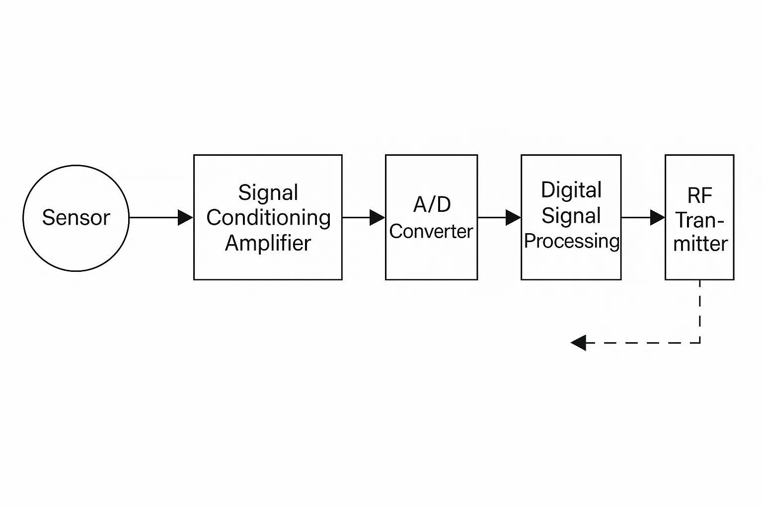
Figure 1 Wearable medical chip system block diagram
1.1 Low-noise Amplifier for Physiological Signal Acquisition
Physiological signals are usually obtained with on-chip biosensors. For ease of integration, sensors use CMOS low-noise amplifiers to convert biological signals into electrical signals. Multiple amplifiers can be integrated for multichannel acquisition of blood pressure, blood oxygen saturation, respiration rate, heart rate, body temperature, and other vital parameters. Because physiological signals are weak and susceptible to environmental noise, amplifiers must provide high sensitivity, high gain, low noise, and low power. A low-pass filter with a cutoff around 1 kHz is commonly used after the amplifier to remove out-of-band noise. Amplifiers can support multiple operating modes such as listen, active, and sleep to reduce overall power consumption.
1.2 Analog-to-Digital Converter (ADC)
Outputs from the front-end multichannel amplifiers are connected to the ADC input via an analog multiplexer that selects one amplifier output at a time. To reduce power consumption, successive-approximation ADCs around 10 bits are commonly chosen. Sigma-delta or pipeline ADCs can offer higher precision and conversion rates, but at the cost of increased power. For wearable medical designs, low power is crucial. Unit capacitors in the ADC must be sized appropriately: too large increases chip area, while parasitic capacitance effects must be minimized.
1.3 Controller
An ARM core or MCU can act as the controller, using a bus to control other circuits, coordinate data timing, configure registers, and manage on-chip communication with other modules.
1.4 Digital Baseband Signal Processing
To improve transmission rate, accuracy, and security, digital outputs from the ADC are processed by a digital baseband processor for compression and encoding. FFT and digital filtering can further remove interference and noise.
1.5 RF Transceiver
Because wearable sensors are placed on different body locations, wired interconnects are inconvenient and prone to tangling. Wireless transmission is the most natural solution. Integrating an RF transceiver on the wearable chip requires different considerations than typical wireless products. Wearable medical systems often use asymmetric transmission: sensors mainly transmit collected physiological data, while received signals are mostly small control commands. Therefore, half-duplex communication is feasible, with low-rate downlink and high-rate uplink. Wearable chips must operate for long periods on small coin cells with voltages around 1.2 to 1.5 V and capacities under a few hundred mA·h. Since the RF section typically dominates power consumption, designers must optimize topology, carrier frequency, transmission method, modulation, data rate, and power consumption to balance low voltage, low power, and sufficient throughput.
2 Wireless Communication Standards for Wearable Medical Chips
Wireless communication technologies evolve rapidly and have driven advances in modern medical technology. Several standards can be used for communication between wearable medical chips. Each standard has characteristics that fit certain use cases but may hinder low-power, short-range wearable applications. The following summarizes the performance and traits of these standards.
2.1 Bluetooth
The Bluetooth standard uses frequency hopping and spread spectrum techniques to suppress intersymbol interference and maintain link quality. It supports approximate ranges of 1, 10, and 100 m and data rates up to 1 Mbps. Bluetooth is simple and cost-effective in mass production. It supports point-to-point serial communication and shared-channel master-controller interfaces, making it suitable for body area network setups. However, Bluetooth operates at 2.4 GHz, a relatively high frequency, and its power consumption can be significant. For some wearable medical use cases, the frequency and power characteristics may not be ideal.
2.2 Zigbee
Zigbee can operate in three bands: 2.4 GHz, 900 MHz, and 800 MHz. Compared with Bluetooth, Zigbee generally consumes less power. At 2.4 GHz it can reach a maximum data rate around 240 kbps. Its limitations include low throughput, higher latency, weaker security, and susceptibility to interference in the crowded 2.4 GHz band.
2.3 UWB
Ultra-wideband (UWB) spans approximately 3.1 to 10 GHz and offers average data rates around 850 kbps, scalable up to 26 Mbps. The standard specifies a power spectral density limit of -41 dBm/MHz but places fewer constraints on time-domain waveforms, allowing impulse-based transmission and simplifying transmitter design. For asymmetric wearable applications where uplink dominates, UWB can reduce power and system complexity by shifting complexity to the receiver. Using wide bandwidth to reduce power makes UWB relatively power-efficient for some use cases.
2.4 WLAN 802.11
IEEE 802.11 WLAN operates in ISM bands. 802.11b and 802.11g run at 2.4 GHz with rates of 11 Mbps and 54 Mbps respectively; 802.11a runs at 5 GHz with up to 54 Mbps. WLAN offers long range and strong interference resistance due to direct-sequence spread spectrum, but its power consumption, complexity, and cost make it unsuitable for most wearable medical chip designs.
2.5 Wireless USB
Wireless USB, like UWB, is based on ultra-wideband and operates from about 3.1 to 10.6 GHz. It supports short-range modes of 3 m and 10 m with data rates up to 480 Mbps and 110 Mbps respectively. Its main challenge for wearable medical applications is power consumption, which limits practical use.
2.6 Infrared Communication (IrDA)
Infrared communication is low-cost and simple, but it requires line-of-sight and point-to-point alignment, and its range and data rates are limited. Compared with Bluetooth and Zigbee, infrared is inconvenient for general wearable data transfer.
2.7 RFID
Radio-frequency identification (RFID) uses magnetic or electromagnetic coupling for contactless data transfer. China has planned RFID bands such as 50–190 kHz, a high-frequency band at 13.56 MHz ±7 kHz, and a 432–434.79 MHz band; other planned bands include 900, 910, and 910.1 MHz, which are widely used for vehicle identification. Like IrDA and Zigbee, RFID is for short-range indoor communication and can support applications such as asset tracking, inventory, patient monitoring, and drug distribution. However, RFID typically has very low data rates and limited security, making it unsuitable for real-time interconnect among wearable medical sensors.
2.8 Body Communication
Body communication, or bio-channel technology, was introduced by Zimmerman at the MIT Media Lab in 1995. Unlike conventional wireless methods, body communication uses the near-body magnetic field or the body itself as the transmission medium. Communication range is typically very short and may require skin contact, allowing precise control of range and endpoints and reducing cross-channel interference while improving security. Near-body wired connections can guarantee high-speed, noise-immune transfers, but wires are inconvenient. Mature wireless technologies such as Zigbee and Bluetooth avoid wires but suffer from low data rates, higher power consumption, and susceptibility to electromagnetic noise. Body communication has therefore attracted attention in research and industry for short-range, secure, low-power wearable links.
3 Development Examples of Wireless Transceivers for Wearable Medical Chips
Driven by microelectronics advances and the needs of aging populations, wearable medical monitoring systems have been developed. A body area network (BAN) consists of many body-worn sensor nodes. Each wireless sensor node can communicate with other nodes or a central node via the wearable chip's wireless transceiver. Early short-range medical monitoring chips used ASK or FSK modulation with low-power crystal oscillators. Those designs could only transmit single vital signs at low rates and had long oscillator startup times, limiting data throughput. Later proposals used inductive-coupling coil communication, but these also suffered from poor link quality and low data rates, reducing communication efficiency and battery life.
Nonstandard systems could not meet the requirements for ultra-low power, tiny size, high reliability, and high data rate. In response, research institutions and chip companies developed more suitable solutions. Representative developments include Zarlink's ZL70101 RF transceiver for medical implants, Toumaz's Sensium system-on-chip, a 2.4 GHz 400 mV low-power transceiver from UC Berkeley researchers, and a body communication transceiver from a Korean research institute.
3.1 Zarlink ZL70101 for Medical Implant Communication
In 2006, Zarlink Semiconductor released the ZL70101, an ultra-low-power, high-performance RF transceiver for medical implant systems. The chip is highly integrated and, excluding matching networks, requires only a single 24 MHz quartz crystal and two decoupling capacitors as three off-chip components. It operates in the 433 MHz ISM band and is fabricated in 0.18 μm RF CMOS. The transceiver current is 5.5 mA during operation and only 250 nA in sleep. The chip integrates a 400 MHz RF transceiver, a 2.45 GHz wake-up signal receiver, and a medium access controller. The receiver uses a low-IF architecture with LNA, image-suppression mixer, IF image-suppression multiphase filter (PPF), RSSI, and ADC. The transmitter includes an up-converter and power amplifier using FSK modulation. The wake-up receiver operates at 2.45 GHz with OOK modulation to detect base-station wake signals and power up the chip, substantially lowering average current. Although designed for implants, its ultra-low power, 2 m range, and up to 800 kbps throughput also suit some wearable interconnect needs.
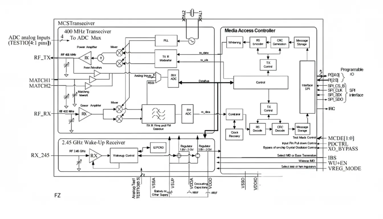
Figure 2 Block diagram of Zarlink MICS RF transceiver
3.2 Toumaz Sensium Low-Power System-on-Chip Transceiver
In 2007, Toumaz released the Sensium SoC integrating an SPI bus, ADC, MCU, RAM, and an ultra-low-power RF transceiver. The RF section occupies about 7 mm2 in 0.13 μm RF CMOS and runs at 1 V. It supports European 870 MHz and U.S. 928 MHz bands. Receive current is 2.1 mA and transmit current is 2.6 mA at -7 dBm output; the transceiver uses half-duplex FSK modulation with a bit error rate around 10^-3 and a data rate of 50 kbps. Sensium targets ECG, pacing, and body temperature telemetry, meeting application requirements. The chip uses a Sliding-IF architecture, which improves image-rejection compared with traditional low-IF designs and reduces DC offset relative to zero-IF structures.
To meet low-power goals, the SoC operates at 1 V, lower than the sum of PMOS and NMOS Vth in 0.13 μm, so many devices—especially analog and RF transistors—operate in subthreshold or weak inversion to reduce power. This complicates RF analog design. The receiver is zero-IF in this implementation, and the system integrates features such as on-chip planar inductors and tunable capacitor matrices for matching. The transmitter’s final driver uses an open-drain NMOS buffer connected to an off-chip LC matching network, requiring thick-gate NMOS devices to prevent breakdown. The VCO operates in self-oscillating mode. Link loss is managed by RSSI-based AGC, and the transmit buffer gain is adjustable to improve power efficiency.
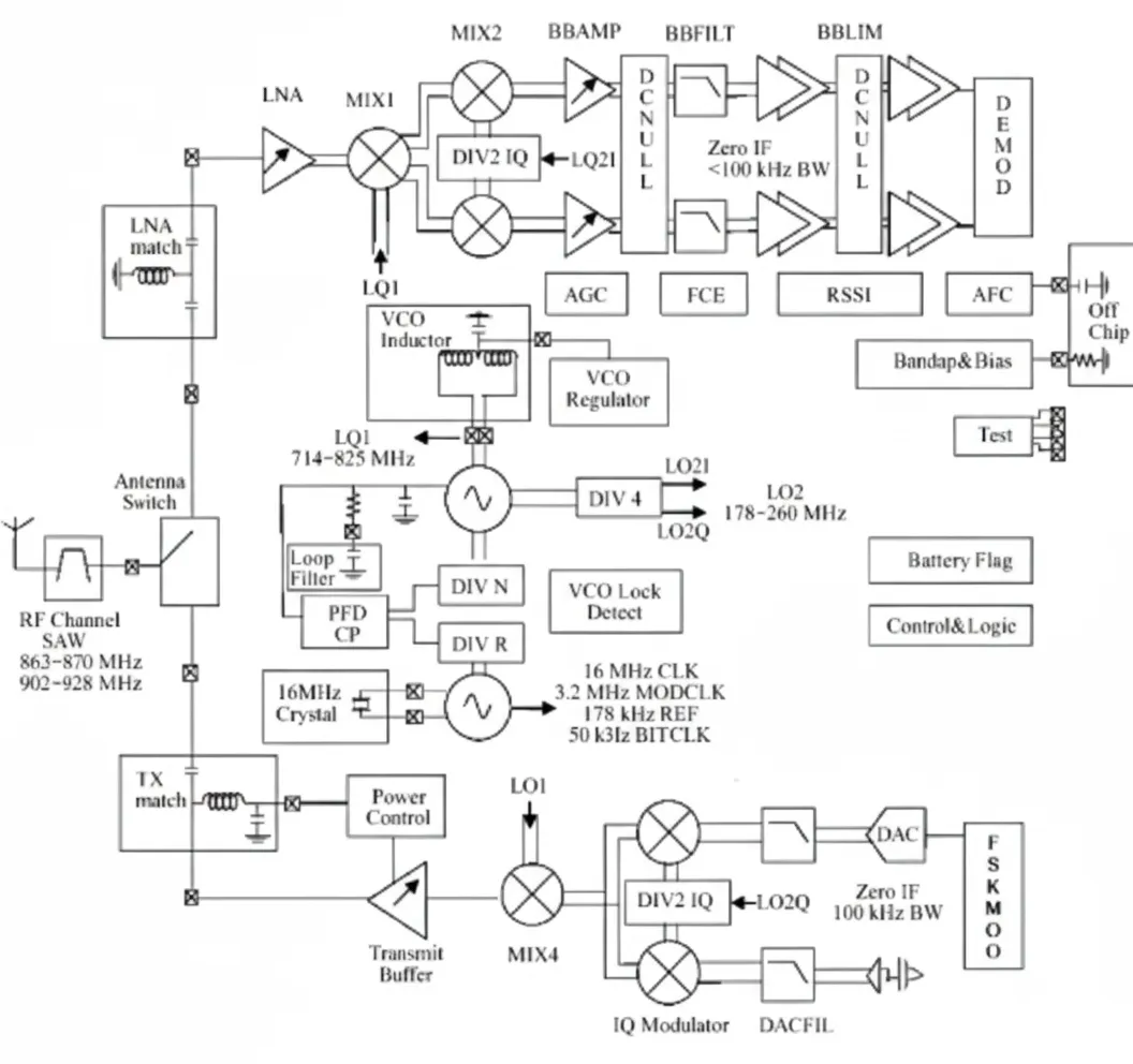
Figure 3 Block diagram of Toumaz RF transceiver
3.3 Body-Communication Based Transceiver Chip
In 2007, a team led by Seong-Jun Son at the Korean Academy of Sciences designed a body-communication transceiver chip that achieved very low power and up to 2 Mbps data rate. The design uses wideband techniques similar to UWB and relies on near-field conduction through the body. The fully digital transceiver operates at 1 V with only 0.2 mW power consumption and occupies 0.85 mm2, making it suitable for short-range, high-rate, ultra-low-power wearable links.
The chip uses body communication principles with operating frequencies from 1 to 200 MHz in a 0.25 μm CMOS process. Only a single signal electrode contacts the skin or clothing, eliminating the need for an additional ground electrode. The transmitter includes a ring oscillator, PRBS generator, and driver buffer. The receiver contains an analog front end amplifier, level shifter, Schmitt trigger, and clock-data recovery (CDR) circuits. To minimize power, the design uses unmodulated direct digital transmission with 200 MHz wideband signaling, fully digital clock recovery, digitally controlled oscillators (DCO), and quadrature sampling. These low-power circuit techniques reduce power in the most consuming blocks such as the front-end amplifier and clock generation.
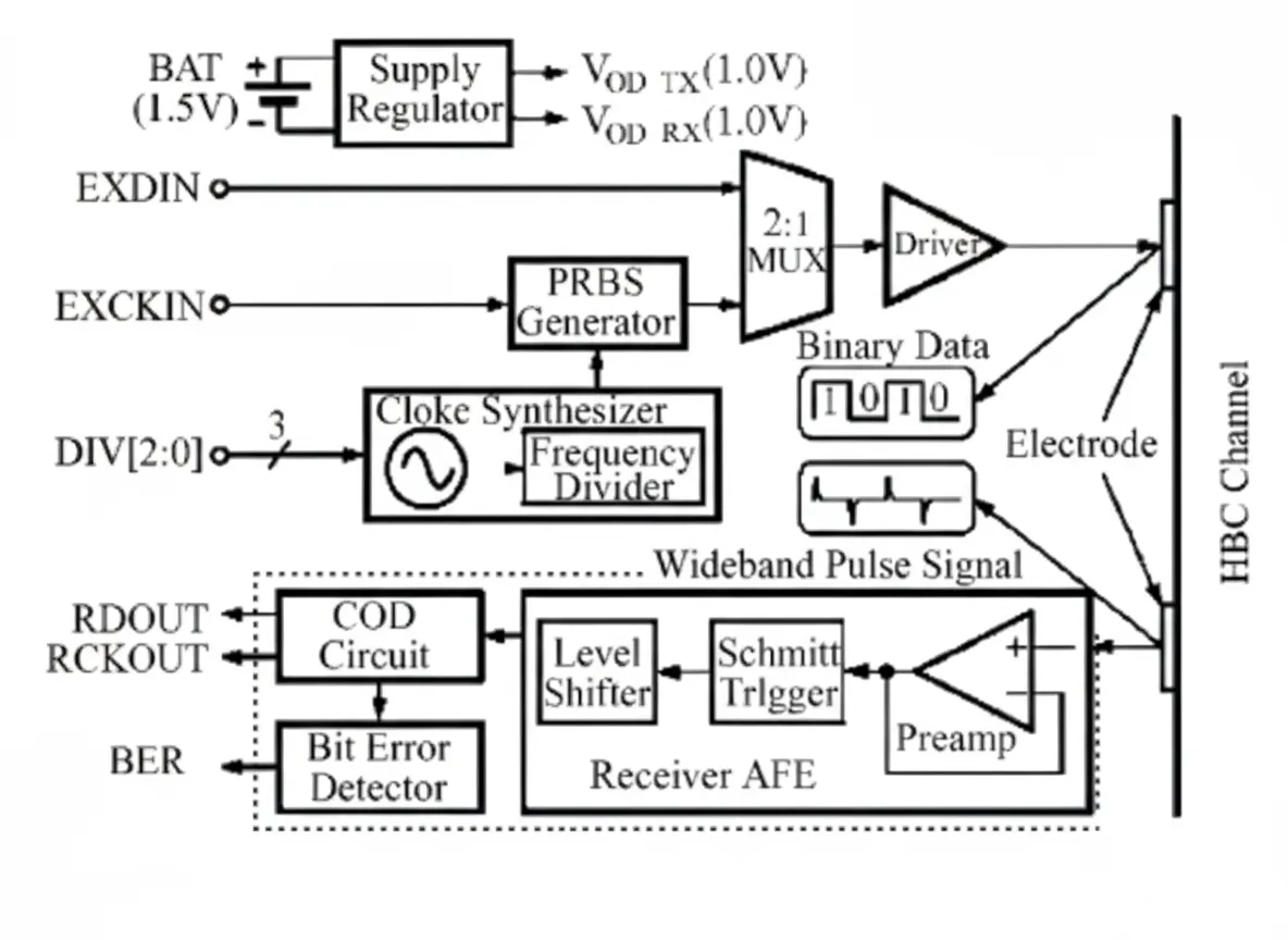
Figure 4 Body communication based transceiver
4 Outlook for Wearable Medical Wireless Transceivers
With increasing stress and rising demands for personal health monitoring, wearable medical chips are gradually integrating into everyday life. Advances in biomedical engineering and microelectronics are driving wearable chips toward miniaturization and networking. Wearable microsystems require sensor nodes to be compact for long-term comfortable wear, and they must transmit physiological signals wirelessly to a central station or other nodes, making networking fundamental. Consequently, future wearable medical chips will trend toward fully integrated SoC solutions to achieve miniaturization and low cost. On-chip RF transceivers will allow sensor node data to be transmitted conveniently and in real time for continuous mobile health monitoring.
No global standard specifically tailored to personal wearable medical systems currently exists. Low-cost, low-power wireless standards in the IEEE 802.15 family are commonly adopted for wearable medical chip development. Although implementations using Zigbee, Bluetooth, or WLAN exist, these protocols were not designed specifically for wearable medical use; their MAC layer and QoS are not optimized for the low-power, high-throughput, short-range characteristics of medical data. Designers still face significant challenges in low-power circuit design and wireless transmission schemes. Many innovative circuit and system concepts require further research and refinement. With continued advances in wireless communication, integrated circuit technology, and market development, these challenges are expected to be addressed, guiding medical monitoring toward lower cost, smaller size, greater intelligence, and improved networking.