ALLPCB


Introduction
Developers can already access MCUs that operate in low-power states, allowing peripherals or even the core to be shut down to reduce system power. However, some applications require more direct control over power consumption to keep parts of the system powered for critical functions.
Historically, designers used discrete power-management components to implement precise power control. In contrast, the ADI ADuCM3029 MCU provides an integrated solution to help designers achieve high performance while minimizing power for sensor data acquisition, wearable electronics, and other IoT applications.
MCU-level power management
For low-power design, engineers can choose from many advanced MCUs with power-saving options. Devices for power-sensitive applications often provide features such as frequency scaling so designers can trade performance for lower power.
Typically, low-power modes reduce power by progressively shutting down MCU subsystems until only the circuits needed to wake the MCU remain active. Ultra-low-power MCUs add special modes that allow separate control of the core and peripheral power, improving power management further. Even so, these modes sometimes shut down peripherals as a group or use automation that grants designers limited control of power allocation details.
Although MCU power management offers a range of low-power modes, moving into low-power mode often reduces functionality significantly. In many cases, applications can tolerate temporary functional loss. However, precise power control is critical for maintaining operation in some applications. The ADuCM3029 processor is designed to support more complex power-management demands in ultra-low-power use cases.
ADuCM3029 overview
The ADuCM3029 is built on an ARM Cortex-M3 core and provides 256 KB of ECC flash and 64 KB of configurable SRAM with parity protection. A variant, the ADuCM3027, offers 128 KB of flash while sharing other features and functions with the ADuCM3029.
Beyond an integrated hardware crypto accelerator, these devices include an 8-channel, 12-bit ADC and multiple digital peripherals, including SPI, I2C, UART, GPIO, synchronous serial ports (SPORT), and a 25-channel DMA controller. Despite the broad feature set, active-mode power is typically under 30 μA/MHz. The ADuCM3029 also enables designers to further tune the balance between functionality, performance, and power.
Fine-grained power tuning
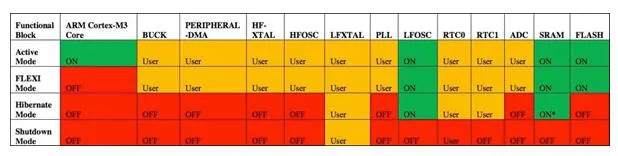
Like most advanced MCUs, the ADuCM3029 offers multiple power modes designed to reduce power during low activity. In sleep mode, the device shuts down the processor core and most peripherals while retaining power to selected SRAM regions; typical power is below 750 nA. In the off mode, the device requires only 60 nA when the application is inactive.
Developers often need some peripherals active while the processor is idle. To address this, the ADuCM3029 provides a Flexi sleep mode. Flexi mode can reduce power to about 300 μA while offering functionality between active and sleep modes. In Flexi mode the core remains in sleep, while developer-selected peripherals stay active.
Developers place the MCU in Flexi mode by clearing the MODE bit in the PMG_PWRMOD register and executing the WFI instruction. With the core idle, specific peripheral functions can be kept enabled by writing 0 to the corresponding bits in the CLKG_CLK_CTL5 register. Although the core cannot execute instructions in this mode, peripherals can continue activities such as DMA transfers between peripherals and memory.
Flexi mode enables keeping peripherals active, which addresses a common sensor-application pattern where one or more sensors must be sampled repeatedly before the processor needs to handle the data. In this scenario developers can use the integrated ADC in automatic cycling mode to perform conversions on selected channels and configure the DMA controller to transfer samples to SRAM. After the programmed number of conversions and associated DMA transfers, the DMA generates an interrupt to wake the core for subsequent sample processing.
Cache and clocks
Flexi mode and other low-power modes provide a powerful mechanism to reduce a design's power at the cost of functionality. For battery-powered systems, designers often require further control. The ADuCM3029 supports a combination of traditional and novel methods to lower power.
Conventionally, an instruction cache reduces accesses to high-energy memory such as off-chip memory or flash. In ADuCM3029-based systems, designers can allocate up to 4 KB of SRAM as a cache. Actual power savings depend on cache hit rate, but using a cache can significantly reduce power in some benchmark applications.
Frequency scaling is another long-term method to reduce power. Lower core clock rates slow instruction execution while reducing power. Unlike many other methods, the ADuCM3029 allows developers to independently adjust clock frequency for the processor and peripherals. The device uses a PLL and clock dividers driven by a 26 MHz internal oscillator or external crystal to generate clocks for on-chip resources, including the processor, memory, and interfaces. A 32 kHz internal oscillator or external crystal drives the real-time clock (RTC) and watchdog timers. Developers can modify clock registers at runtime to change clock frequency to meet changing application requirements or to exploit power-reduction opportunities.
Enhanced power path
In addition to traditional power-reduction methods, the ADuCM3029 offers a novel approach based on dedicated on-chip hardware. The power path includes an on-chip buck converter to reduce the gap between the device supply voltage VBAT (1.74 V–3.6 V) and the internal digital domain operating voltage (1.2 V).
Under normal operation, the internal 1.2 V is supplied by an integrated LDO. As with any typical LDO, when the difference between the LDO input and load voltage is large, the default power path dissipates excess energy, causing power loss. With this MCU, designers can reduce that loss at higher supply voltages by adding a small number of external capacitors and enabling the buck converter in software by writing to the PMG_CTL1 register.
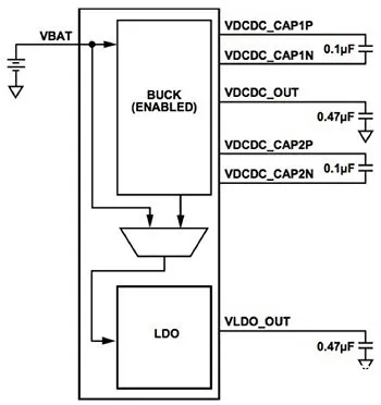
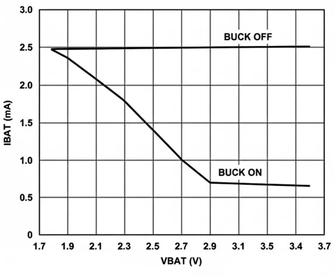
The converter uses an efficient capacitor-based charge-pump topology to lower the voltage delivered to the LDO, reducing power consumption at higher VBAT voltages. When VBAT falls below about 2.3 V, the buck converter bypasses and follows VBAT.
Power-optimized sampling
Features such as cache, frequency scaling, and on-chip DC-DC conversion operate at the system level to lower power. At the application level, functions such as Flexi mode reduce power consumed by peripheral operations like sensor sampling. Yet even with these methods, some applications may still need further savings. Battery-powered IoT devices often sample sensors at very low rates or monitor an external process periodically.
For slow periodic activity, developers typically use the MCU RTC for a consistent timebase and a countdown timer to wake the MCU at precise scheduled times. Advanced MCUs commonly retain RTC functionality in very low-power modes. The ADuCM3029 provides two independent RTCs, RTC0 and RTC1, offering more options for balancing power and performance.
Both RTCs operate in active, Flexi, and sleep modes, but only RTC0 remains available in the lowest-power off mode. The differences between the two clocks enable more complex timing schemes. RTC0 counts time in seconds (1 Hz) and is therefore limited to wake times specified in whole seconds. RTC1 supports a wider range of prescaling and can provide wake times down to 30.7 μs. Each clock also consumes different power: RTC0 is powered from VBAT, while RTC1 is powered from the internal 1.2 V domain. Using the optional buck converter can further reduce RTC1 effective power. RTC1 also supports Analog Devices' SensorStrobe mechanism, a built-in low-power sampling feature in the ADuCM3029.
SensorStrobe is a special RTC1 alarm that generates an output pulse on the MCU's RTC1_SS1 pin. Developers can connect the ADuCM3029 SensorStrobe output to a multi-sensor device such as the ADXL363 to implement a low-power sampling solution with a small external component count.
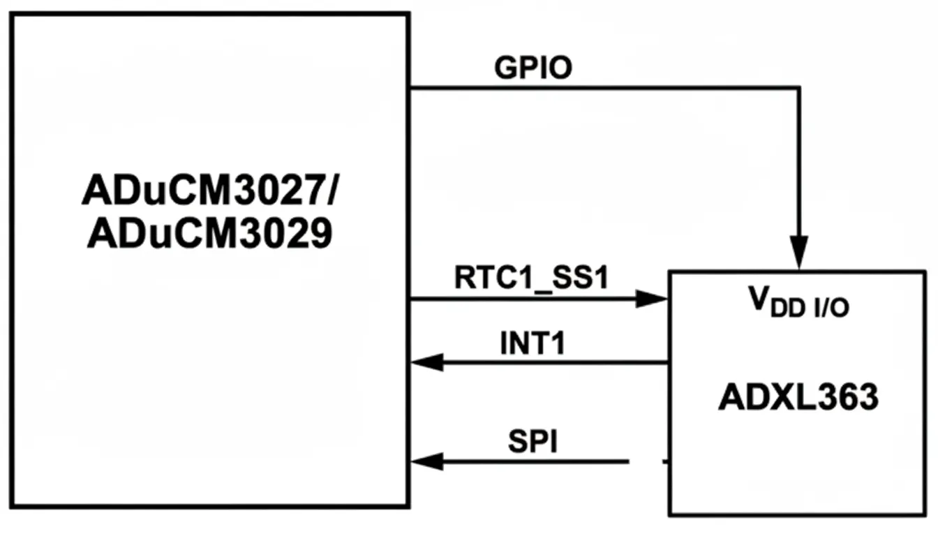
The ADuCM3029 EZ-KIT development board includes this subsystem. Beyond simple hardware wiring, the mechanism can be configured with a few register writes to start SensorStrobe operation.
While SensorStrobe is running, the ADuCM3029 can be placed in sleep mode to minimize MCU power during extended sampling. With the MCU in sleep, RTC1 counts to the value set during SensorStrobe configuration. When the SensorStrobe count condition is met, the SensorStrobe signal is asserted to the ADXL363 interrupt input to wake that device. The ADXL363 performs its sampling routine and then signals the MCU interrupt pin to wake the MCU and begin processing the sampled data.
Previously, designers often used an external RTC, timers, or simple oscillators for extended sampling designs. Besides increasing design complexity, external clock sources break time synchronization between sampled data and the MCU timebase, requiring data resampling to align timestamps. Using RTC1 with SensorStrobe ensures sampling timestamps remain synchronized with the ADuCM3029-based system.
Conclusion
The demand for lower-power systems continues to challenge designers to deliver high performance in smaller, energy-efficient designs. Each application requires a specific balance between functionality and power, increasing design complexity.
The integrated power-management features of the ADuCM3029 MCU give developers flexible options to implement such balances. Using this device, designers can more easily meet the unique performance and low-power requirements of their applications.