 ALLPCB


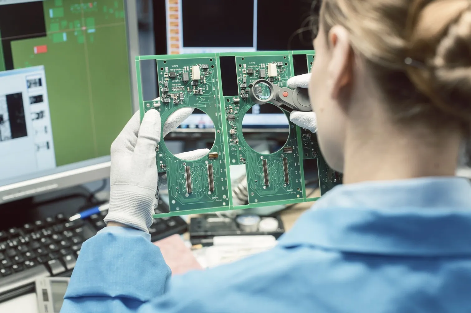
Introduction
Printed circuit boards form the backbone of modern electronics, where manufacturing precision directly impacts device reliability and performance. Engineers frequently face defects like PCB solder bridging, lifted pads in PCBs, PCB trace damage, cold solder joints needing repair, and black pad defects during production runs. These issues can lead to assembly failures, field returns, or safety risks if not addressed promptly. Identifying root causes requires a systematic approach rooted in factory processes and quality control measures. This practical guide equips electrical engineers with troubleshooting strategies, drawing from established manufacturing insights to minimize downtime and enhance yield rates. By focusing on common defects, it emphasizes prevention and correction techniques suitable for high-volume production environments.
The Impact of PCB Manufacturing Defects on Production
Defects in PCB manufacturing disrupt the supply chain and increase costs through rework or scrap. For instance, even minor issues like PCB trace damage can cascade into functional failures under operational stress. Industry data highlights that early detection during inspection phases prevents escalation to assembly stages. Engineers must prioritize visual, electrical, and automated optical inspections to catch these early. Aligning troubleshooting with standards such as IPC-A-600 ensures consistent acceptability criteria across facilities. Ultimately, mastering these defects supports scalable production while upholding product integrity.
PCB Solder Bridging: Causes and Identification
PCB solder bridging occurs when excess solder paste connects adjacent pads or leads during reflow soldering, creating unintended electrical shorts. Common causes include stencil misalignment, excessive solder paste volume, or improper reflow profiles that fail to collapse bridges before solidification. In high-density surface-mount technology assemblies, pad spacing below 0.5 mm exacerbates the risk due to paste flow dynamics. Engineers can identify bridges through shiny solder filaments between pins under magnification or via flying probe testing for continuity faults. Factory-driven prevention starts with optimizing stencil apertures to control deposit thickness. Regular profilometer checks on stencils maintain aperture integrity over print cycles.
Troubleshooting and Repairing PCB Solder Bridging
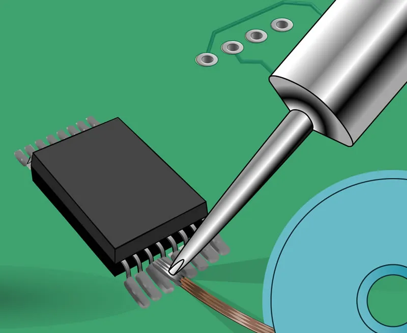
To repair PCB solder bridging, begin by isolating the board electrically and using a hot air rework station at controlled temperatures to wick away excess solder with braided copper. Avoid mechanical scraping, which risks pad damage or residue contamination. Post-repair, perform inter-pad resistance measurements exceeding 1 megaohm to verify isolation. For prevention, implement solder paste release agents and validate reflow oven zoning per J-STD-001 requirements for uniform heating. Engineers should audit paste printer setups daily, correlating print defects with bridging incidence rates. This methodical approach reduces recurrence in subsequent panels.
Lifted Pads in PCBs: Mechanisms and Detection
Lifted pads in PCBs manifest as delaminated copper foil from the substrate, often during soldering or drilling operations. Excessive heat from wave soldering or multiple reflow passes weakens adhesive bonds, especially on thinner boards with high Tg laminates. Mechanical stress from component insertion or poor drill exit quality contributes by fracturing the pad-barrel interface. Detection involves cross-section microscopy revealing voiding or fiber pullout at the lift site. IPC-A-600 class guidelines classify lifted pads as reject criteria based on lift height and functionality impact. Factory quality control teams use automated X-ray for hidden lifts under components.
Solutions for Lifted Pads PCB Issues
Addressing lifted pads PCB problems requires immediate jumper wire installation using 0.1 mm insulated wire bonded with conductive epoxy, followed by conformal coating for strain relief. For production prevention, select drill parameters matching board thickness and copper weight to minimize burrs. Engineers benefit from implementing via-in-pad designs cautiously, ensuring annular ring widths comply with fabrication tolerances. Thermal profiling during assembly simulates multiple reflows to qualify process windows. Post-drill deburring with plasma or chemical etchants preserves pad adhesion. These steps align factory workflows with reliable pad retention.
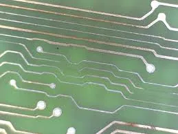
PCB Trace Damage: Origins and Assessment
PCB trace damage appears as nicks, cracks, or etches into copper conductors, compromising current carrying capacity and signal integrity. Etching undercuts from over-etch solutions or misalignment of dry film photoresist cause narrow traces prone to fracturing. Handling during shipping or fixturing introduces mechanical dents, particularly on fine-pitch flex circuits. Assessment combines continuity testing with microscope examination for constriction points below specified widths. Trace resistance calculations help quantify damage severity relative to design current ratings. In manufacturing, etch factor monitoring prevents excessive lateral undercut.
Repairing and Preventing PCB Trace Damage
Repair PCB trace damage by milling a slot and embedding a zero-ohm jumper or conductive ink trace, then encapsulating with epoxy. Verify repair conductivity matches original trace specs through four-wire kelvin measurements. Prevention involves conveyor edge supports to avoid board flexure and cleanroom handling protocols. Engineers should specify trace etch control in fab drawings, targeting uniform developer spray patterns. Panel-level stress testing simulates assembly forces early. Consistent application yields traces resilient to downstream processes.
Cold Solder Joints: Characteristics and Root Causes
Cold solder joints exhibit a dull, grainy appearance with poor wetting, resulting from insufficient reflow temperature or rapid cooling rates that trap flux residues. Inadequate preheat fails to activate flux fully, leading to incomplete intermetallic formation between solder and pad finish. Vibration during solidification or contaminated pads from oils further degrade joint strength. Electrical symptoms include intermittent connectivity under thermal cycling. J-STD-001 defines acceptable fillet shapes and wetting coverage for class 3 assemblies. Factories track oven thermocouple data to correlate profiles with joint quality.
Cold Solder Joint Repair Techniques
Cold solder joint repair starts with flux application and localized reheating to 250 degrees Celsius using a soldering iron with temperature control. Mechanically disturb the joint gently to reflow solder, ensuring convex meniscus formation. Clean residues with isopropyl alcohol and inspect for 100% pad coverage. For prevention, validate nitrogen reflow atmospheres to suppress oxidation and preheat ramps at 1-2 degrees Celsius per second. Engineers integrate in-line thermal imaging for real-time profile adjustments. This ensures robust joints across production lots.
Black Pad Defect: Formation and Diagnosis
Black pad defect plagues electroless nickel immersion gold (ENIG) finishes, where nickel corrosion creates a non-wettable black oxide layer beneath gold. Hyper-corrosion during immersion gold plating stems from high phosphorus nickel or acidic bath imbalances. The defect evades visual detection until reflow reveals dewetting with solder balls. Cross-sectional analysis via scanning electron microscopy confirms nickel pits exceeding 50% surface area. It predominantly affects fine-pitch pads in high-reliability applications. Manufacturing controls focus on bath chemistry stability and phosphorus content between 7-9%.
Mitigating Black Pad Defect in Production
Mitigate black pad defect by switching to alternative finishes like organic solderability preservative for cost-sensitive boards or immersion tin with controlled displacement. In ENIG processes, monitor pH daily and use palladium activation to enhance nickel integrity. Post-plating adhesion tests per tape pull methods screen panels early. Engineers qualify vendors through accelerated aging simulations matching end-use environments. Implementing these reduces black pad incidence below 0.1% in qualified lines. Factory SPC charts track defect trends for continuous improvement.
Integrated Quality Control Strategies
A holistic quality control framework combines automated optical inspection with electrical test fixtures tailored to detect multiple defects simultaneously. Engineers develop failure mode effects analysis prioritizing high-risk processes like reflow and etching. Supplier audits ensure laminate and finish consistency. Training operators on defect recognition per IPC classes accelerates yield ramps. Data analytics from manufacturing execution systems predict defect hotspots. This proactive stance minimizes common issues across the board lifecycle.
Conclusion
Troubleshooting PCB manufacturing defects demands a blend of technical insight and process discipline, targeting issues like PCB solder bridging, lifted pads PCB, PCB trace damage, cold solder joint repair, and black pad defect. Engineers armed with these strategies achieve higher first-pass yields and reliable assemblies. Adhering to standards fosters consistency in factory outputs. Regular process audits and team training sustain improvements. Ultimately, these practices elevate PCB quality, supporting innovative electronics design.
FAQs
Q1: What causes PCB solder bridging and how can engineers prevent it?
A1: PCB solder bridging arises from excess paste, stencil misalignment, or improper reflow profiles. Prevention involves optimizing stencil thickness to 100-125 microns, validating paste volume via SPI, and zoning ovens for peak temperatures above 235 degrees Celsius. Regular maintenance of printers and post-print inspections reduce occurrences significantly in SMT lines.
Q2: How do you identify and repair lifted pads PCB?
A2: Lifted pads PCB show delamination from heat or drilling stress, detected by visual or X-ray inspection. Repair uses conductive epoxy jumpers with strain relief coating. Prevention includes drill parameter optimization and thermal profiling for assemblies. IPC-A-600 criteria guide acceptability decisions.
Q3: What are the steps for cold solder joint repair?
A3: Cold solder joint repair requires fluxing, reheating to full reflow, and verifying wetting. Root causes include poor preheat or contamination. J-STD-001 outlines fillet requirements. In-line thermal monitoring prevents issues in production.
Q4: How to troubleshoot black pad defect in PCB manufacturing?
A4: Black pad defect from ENIG corrosion shows as dewetting. Diagnose via cross-section SEM and mitigate with bath controls or alternative finishes. Phosphorus nickel optimization and adhesion tests are key. Factory SPC tracks reliability.
References
IPC-A-600K — Acceptability of Printed Boards. IPC, 2020
J-STD-001H — Requirements for Soldered Electrical and Electronic Assemblies. IPC, 2018


