 ALLPCB


Introduction
Microvias play a critical role in high-density interconnect (HDI) printed circuit boards, enabling compact designs for advanced electronics like smartphones and medical devices. These small vias, typically laser-drilled and less than 150 microns in diameter, allow for tighter routing and more layers without increasing board size. However, designing PCBs with microvias introduces unique challenges that can lead to reliability issues if not addressed properly. Common pcb design mistakes, such as overlooking fabrication limits, often result in costly rework or field failures. This article outlines the top five microvia errors to avoid, providing logical engineering explanations and design tips for electrical engineers. By understanding these pitfalls, you can enhance hdi design flaws prevention and improve overall pcb troubleshooting efficiency.
What Are Microvias and Why Do They Matter in PCB Design?
Microvias are blind or buried vias with small apertures, formed by laser ablation or plasma etching to connect adjacent layers in multilayer boards. They differ from standard through-holes by their reduced size, which supports higher component density and finer pitch interconnects essential for modern high-speed circuits. In HDI PCBs, microvias enable via-in-pad technology and staggered configurations, reducing signal path lengths and minimizing inductance. Their importance grows with the demand for miniaturization, but they demand precise control over drilling, plating, and lamination processes. Failures like cracking or delamination can compromise signal integrity and thermal performance, making microvia reliability a key factor in product lifespan. Electrical engineers must prioritize these elements to meet performance targets in compact assemblies.
Mistake 1: Exceeding Recommended Aspect Ratios
One prevalent error in microvia design involves ignoring aspect ratio limits, where the via's depth exceeds allowable proportions relative to its diameter. High aspect ratios complicate electroplating, leading to voids or thin copper walls that fail under thermal cycling. IPC-2226 guidelines specify maximum ratios to ensure uniform plating and structural integrity. Engineers often push boundaries for density, but this risks incomplete fill and electromigration issues during operation. The result is higher resistance and potential open circuits, especially in power delivery networks. To mitigate, always calculate ratios early in the stackup phase and verify against design rules.
This mistake stems from mismatched dielectric thicknesses and via sizes during initial layout. Laser-drilled holes in thin cores demand ratios below 1:1 for reliability, as deeper vias trap plating solutions poorly. Simulations show stress concentrations amplify at higher ratios, accelerating fatigue. Practical design tips include selecting thinner dielectrics or wider apertures where possible. Cross-checking with fabrication capabilities prevents surprises in production. Consistent adherence reduces microvia errors significantly.
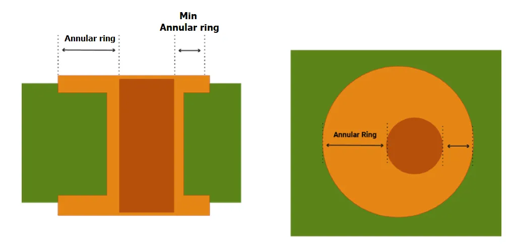
Mistake 2: Inadequate Annular Ring Specifications
Insufficient annular ring sizes around microvias represent another critical hdi design flaw, often overlooked in pursuit of minimal footprints. The annular ring provides the landing area for plating and supports mechanical stress during assembly. Too small a ring leads to pad breakout or lift-off under solder reflow conditions. Standards like IPC-6012DS emphasize minimum dimensions to accommodate drill tolerances and expansion. Engineers may default to aggressive rules without considering misalignment from sequential lamination. This error manifests as intermittent connections, complicating pcb troubleshooting post-assembly.
Fabrication processes introduce variations in laser positioning and copper etching, necessitating buffer zones. A narrow ring exacerbates CTE mismatches between copper and dielectric, promoting cracks at interfaces. Design reviews should enforce rulesets with at least 50% oversize relative to via diameter. Stacked microvias compound the issue, requiring even larger rings on inner targets. Implementing via tents or fills enhances robustness. Proactive sizing aligns design intent with manufacturability.
Mistake 3: Improper Via Stacking and Configuration
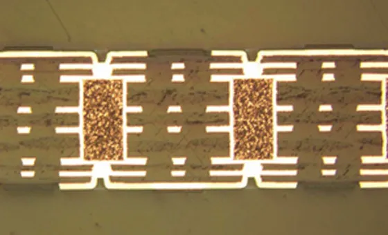
Stacking microvias without staggering or limiting layers per structure invites alignment errors and reliability failures. Stacked configurations, where vias align vertically across multiple layers, concentrate stress and hinder plating uniformity. Preferred practices favor staggered or offset placements to distribute loads and improve fill. Over-reliance on stacked vias for cost savings ignores their higher failure rates under thermal excursion. This pcb design mistake appears in high-layer-count boards, causing barrel cracks or target pad separation. Early stackup planning prevents these microvia errors.
Mechanical drilling for through-vias combined with laser microvias demands precise registration during build-up. Misalignment accumulates across layers, weakening interconnects. IPC-TM-650 test methods highlight cycling endurance limits for stacked vs. staggered. Electrical engineers benefit from modeling via farms with simulation tools for stress analysis. Opt for any-layer vias only when density justifies added complexity. Balanced configurations ensure long-term performance.
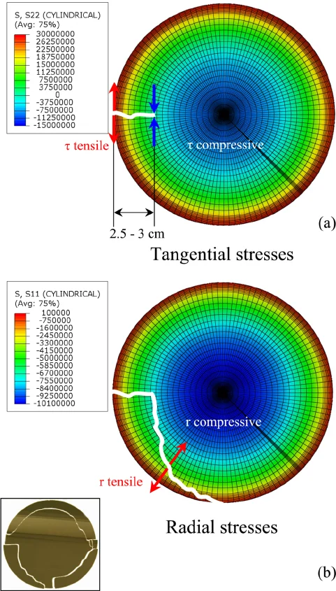
Mistake 4: Neglecting Thermal Management and CTE Mismatch
Overlooking coefficient of thermal expansion (CTE) differences between materials leads to microvia failures from warpage and delamination. Dielectrics and copper expand at varying rates during reflow or operation, stressing via barrels. High-power designs amplify heat, exacerbating microcracks at pad interfaces. This common oversight in dense layouts ignores the need for low-CTE resins in HDI cores. Resulting issues include voiding and reliability drops, demanding extensive pcb troubleshooting. Integrating thermal vias and balanced stackups counters these effects.
Heat dissipation paths must incorporate microvias thoughtfully to avoid hotspots. Simulations reveal peak stresses at via corners under mismatch. Material selection favors resin systems with matched CTE to copper foil. Layer symmetry in the stackup minimizes bow and twist. Monitoring junction temperatures guides via placement. Comprehensive analysis upholds design integrity.
Mistake 5: Skipping Design for Manufacturability Checks
Failing to consult fabricator capabilities early results in unbuildable designs, a top pcb design mistake with microvias. Assumptions about drill sizes, plating chemistries, or lamination sequences mismatch real processes. Without DFM reviews, features like tight spacing or deep stacks trigger yield losses. Sequential build-up for HDI requires validated parameters from suppliers. This error delays prototypes and inflates costs. Structured checklists and iterative feedback loops resolve it effectively.
Capabilities vary by facility, affecting microvia aspect ratios and fill methods. Pre-tapeout audits catch discrepancies in rules files. Collaboration ensures compliance with process windows. Post-design simulations validate signal and power integrity alongside fab rules. Thorough vetting streamlines production.
Practical Solutions and Best Practices
Adopting structured workflows elevates microvia designs. Start with stackup optimization, prioritizing symmetry and material compatibility. Enforce DRCs tailored to HDI, including via-to-via spacing and ring controls. Simulate thermal-mechanical behavior to predict failures. Prototype iteratively with fab partners for validation. These design tips minimize hdi design flaws and enhance reliability.
Layer pairing reduces via count, easing routing congestion. Filled vias in pad sites improve planarization for fine-pitch BGA. Documentation of assumptions aids troubleshooting. Regular training on standards keeps teams aligned.
Troubleshooting Insights for Electrical Engineers
When microvia issues arise, inspect for plating voids via cross-sectioning. Thermal cycling tests per IPC methods reveal latent weaknesses. Signal probing identifies high-resistance paths. Root cause analysis traces back to design rules. Corrective actions refine future iterations. Logical deduction streamlines resolution.
Conclusion
Avoiding these top five mistakes—aspect ratio excesses, ring inadequacies, poor stacking, thermal neglect, and DFM oversights—fortifies microvia PCB designs. Logical adherence to engineering principles and standards ensures robust HDI performance. Electrical engineers gain from proactive planning and validation. Implement these pcb troubleshooting strategies for superior outcomes. Reliable boards drive innovation without compromise.
FAQs
Q1: What are the most common pcb design mistakes with microvias?
A1: Exceeding aspect ratios and inadequate annular rings top the list, as they compromise plating and mechanical strength. Stacked via misalignment and CTE mismatches follow, leading to cracks under stress. Early DRC enforcement and fab consultation prevent these microvia errors effectively. Structured stackups further bolster reliability.
Q2: How can engineers avoid hdi design flaws in microvia layouts?
A2: Prioritize staggered configurations over stacked for better stress distribution. Verify material CTE compatibility to mitigate thermal failures. Use simulation for via farm analysis and enforce IPC-guided dimensions. Iterative DFM reviews align designs with fabrication limits, reducing risks.
Q3: What design tips improve microvia reliability?
A3: Opt for lower aspect ratios and larger rings to enhance plating uniformity. Balance stackups symmetrically to control warpage. Integrate thermal vias for heat paths and validate via cycling endurance. These practices minimize pcb troubleshooting needs.
Q4: Why do microvia errors occur during PCB manufacturing?
A4: Misalignment from lamination and plating voids from high ratios are primary culprits. Thermal expansion mismatches cause delamination post-reflow. Preemptive rule checks and material selection address root causes, ensuring high yields.
References
IPC-2226A — Sectional Design Standard for High Density Interconnect (HDI) Printed Boards. IPC, 2003
IPC-6012DS — Qualification and Performance Specification for High Density Interconnect (HDI) Printed Boards. IPC, 2015
IPC-TM-650 — Test Methods Manual. IPC, 2020


