 ALLPCB


Designing a printed circuit board (PCB) with an optimal layer stackup is crucial for ensuring signal integrity, minimizing noise, and achieving reliable performance in modern electronics. If you're searching for guidance on PCB layer stackup software, controlled impedance layer stackup, or multilayer PCB design software, this comprehensive guide will walk you through the essentials of layer stackup design. From understanding dielectric constants to calculating layer thickness, we’ve got you covered with practical tips and actionable insights.
In this ultimate guide, we’ll dive deep into the process of designing a layer stackup using specialized tools, explore the importance of controlled impedance, and provide step-by-step advice for achieving a balanced and high-performing PCB design. Whether you're a beginner or an experienced engineer, this blog will equip you with the knowledge to tackle complex multilayer designs with confidence.
What is PCB Layer Stackup and Why Does It Matter?
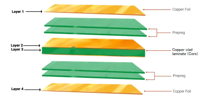
A PCB layer stackup refers to the arrangement of copper layers and insulating materials (dielectrics) that make up a circuit board. This structure determines how signals travel, how power is distributed, and how well the board can handle electromagnetic interference (EMI). A well-designed stackup is the foundation of a successful PCB, especially for high-speed or high-frequency applications.
Why is layer stackup design so important? It directly impacts signal integrity, impedance control, and overall board performance. A poorly planned stackup can lead to issues like crosstalk, signal delays, or even complete circuit failure. By using PCB layer stackup software, engineers can visualize and optimize the arrangement of layers before manufacturing, saving time and reducing costly errors.
Key Components of a PCB Layer Stackup
Before diving into the design process, let’s break down the key components of a layer stackup:
- Signal Layers: These layers carry electrical signals between components. They are often placed on the outer layers or inner layers, depending on the design.
- Ground Planes: These are dedicated copper layers that provide a reference for signals and help reduce noise and EMI.
- Power Planes: These layers distribute power to components, ensuring stable voltage levels across the board.
- Dielectric Layers: Insulating materials between copper layers, characterized by their dielectric constant (Dk), which affects signal speed and impedance.
Understanding these elements is critical when using multilayer PCB design software to arrange layers for optimal performance.
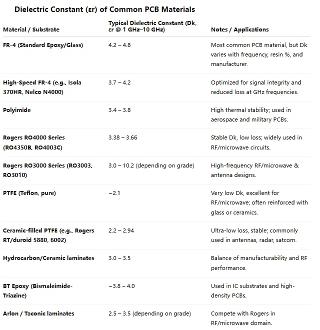
The Role of Dielectric Constant in PCB Design
The dielectric constant (Dk) of a material measures its ability to store electrical energy in an electric field. In PCB design, it influences how fast signals travel through the board and how impedance is managed. Common materials like FR-4 have a Dk value of around 4.2 to 4.5 at 1 MHz, while high-frequency materials might have lower values for faster signal transmission.
A higher dielectric constant slows down signal propagation, which can be a concern in high-speed designs. When designing a stackup, you must select materials with appropriate Dk values to match your application’s needs. For instance, in high-frequency circuits operating above 1 GHz, choosing a material with a lower Dk (e.g., 3.0) can minimize signal delay and loss.
Understanding Controlled Impedance in Layer Stackup Design
Controlled impedance layer stackup is a critical aspect of high-speed PCB design. Impedance refers to the resistance a signal encounters as it travels through a trace, and maintaining consistent impedance (often 50 ohms for single-ended signals or 100 ohms for differential pairs) is essential to prevent signal reflections and ensure data integrity.
To achieve controlled impedance, you need to carefully design the trace width, layer thickness, and dielectric properties. For example, a typical 50-ohm microstrip on an FR-4 substrate with a dielectric thickness of 0.2 mm might require a trace width of approximately 0.3 mm. These calculations can be complex, but PCB layer stackup software often includes built-in calculators to simplify the process.
Proper impedance control starts with a well-planned stackup. Ground planes should be placed close to signal layers to provide a stable reference, and dielectric thickness must be consistent to avoid impedance mismatches. Failing to account for these factors can result in signal degradation, especially in applications like USB, HDMI, or Ethernet.
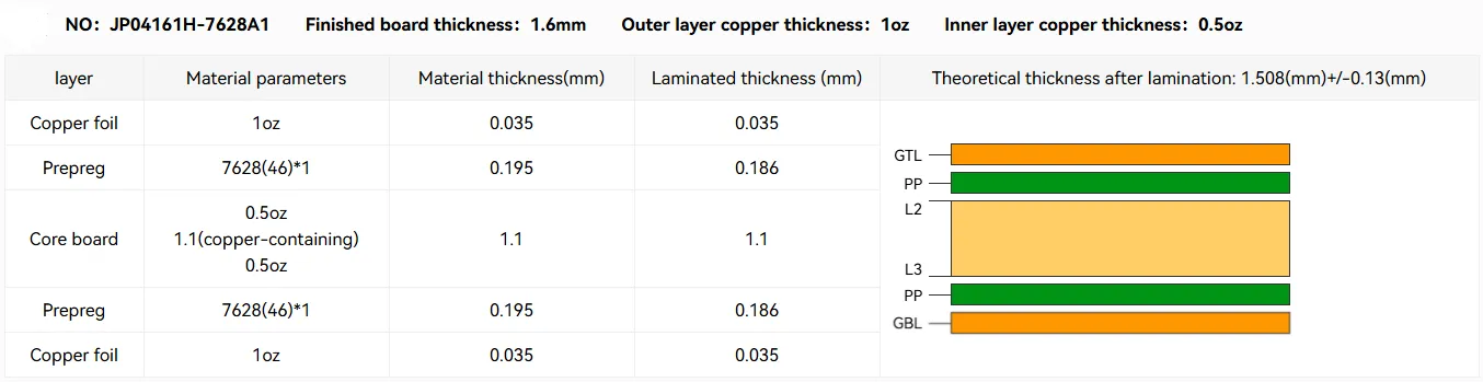
How to Perform PCB Layer Thickness Calculation
Determining the right layer thickness is a key step in stackup design. The PCB layer thickness calculation depends on several factors, including the type of signal, frequency, and manufacturing constraints. Here’s a basic approach to calculating thickness:
- Define Signal Requirements: High-speed signals often require thinner dielectric layers to maintain impedance and reduce signal loss.
- Consider Manufacturing Limits: Standard PCB thicknesses range from 0.8 mm to 1.6 mm for the entire board, with individual dielectric layers as thin as 0.1 mm.
- Use Software Tools: Many design platforms include features to simulate and calculate optimal layer thickness based on your impedance goals.
For instance, if you’re designing a 4-layer PCB with a total thickness of 1.6 mm, you might allocate 0.2 mm for each dielectric layer and 0.035 mm for each copper layer, leaving room for prepreg and core materials. Adjusting these values can help balance cost, performance, and manufacturability.
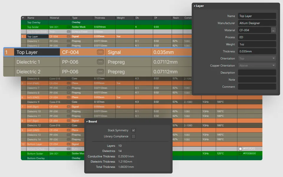
Steps to Design a Layer Stackup Using PCB Software
Designing a layer stackup can seem daunting, but with the right multilayer PCB design software, the process becomes manageable. Follow these steps to create an effective stackup:
Step 1: Define Your Layer Count
Start by determining how many layers your design needs. A simple circuit might work with 2 or 4 layers, while complex high-speed designs may require 8, 10, or more. Each additional layer increases cost, so balance performance with budget.
Step 2: Arrange Signal, Power, and Ground Layers
Place ground and power planes strategically to minimize noise. A common practice for a 4-layer board is to use the top and bottom for signals, with inner layers dedicated to ground and power. For more layers, alternate between signal and plane layers to maintain symmetry.
Step 3: Set Dielectric and Copper Thickness
Input the dielectric and copper thicknesses based on your impedance requirements and manufacturing capabilities. Use software tools to simulate how these values affect signal performance.
Step 4: Simulate and Optimize for Impedance
Use the software’s impedance calculator to ensure traces meet target values (e.g., 50 ohms). Adjust trace widths and layer spacing as needed to achieve a controlled impedance layer stackup.
Step 5: Validate the Design
Run simulations to check for signal integrity issues, crosstalk, or EMI. Most advanced software offers built-in analysis tools to identify potential problems before manufacturing.
Best Practices for Multilayer PCB Stackup Design
To ensure your multilayer PCB performs as expected, follow these best practices:
- Maintain Symmetry: Keep the stackup symmetrical to avoid warping during manufacturing. For example, in an 8-layer board, pair signal and plane layers evenly on both sides of the center.
- Minimize Layer Transitions: Route high-speed signals on a single layer when possible to avoid vias, which can introduce impedance discontinuities.
- Choose Materials Wisely: Select dielectric materials with consistent dielectric constant (Dk) values across the frequency range of your application.
- Plan for Thermal Management: Allocate thicker copper layers or additional planes for heat dissipation in high-power designs.
Common Challenges in Layer Stackup Design and How to Overcome Them
Even with the best tools, challenges can arise during stackup design. Here are some common issues and solutions:
- Impedance Mismatch: If simulations show inconsistent impedance, adjust trace widths or dielectric thickness. Use software calculators to fine-tune values.
- Crosstalk: Separate high-speed signal layers with ground planes to reduce interference. Ensure adequate spacing between traces on the same layer.
- Manufacturing Constraints: Work closely with your fabrication partner to confirm layer thicknesses and material availability early in the design process.
Why Use PCB Layer Stackup Software?
Modern PCB layer stackup software is a game-changer for engineers. These tools allow you to visualize layer arrangements, calculate impedance, and simulate signal behavior before building a prototype. Benefits include:
- Accuracy: Built-in calculators ensure precise PCB layer thickness calculation and impedance matching.
- Efficiency: Automated features reduce design time and minimize errors.
- Cost Savings: Identifying issues during the design phase prevents expensive revisions after manufacturing.
Conclusion: Mastering Layer Stackup Design for Better PCBs
Layer stackup design is a critical step in creating high-performing PCBs, especially for complex multilayer boards. By leveraging multilayer PCB design software, understanding the role of dielectric constant (Dk), and following best practices for controlled impedance layer stackup, you can ensure your designs meet performance and reliability standards.
Whether you’re calculating layer thicknesses or arranging signal and ground planes, the right tools and knowledge make all the difference. Use this guide as your roadmap to mastering stackup design, and take your PCB projects to the next level with confidence.
With a solid foundation in layer stackup principles and the power of advanced software, you’re well-equipped to tackle even the most challenging designs. Keep experimenting, simulating, and optimizing to achieve the best possible results for your next project.


