 ALLPCB


Effective PCB component placement is the foundation of a high-performing printed circuit board design. By strategically positioning components, you can maximize performance, reduce noise, and ensure signal integrity, especially in high-speed applications. In this comprehensive guide, we’ll explore proven placement strategies, noise reduction techniques, and component orientation tips to help you achieve optimal results in your PCB designs.
Whether you're working on a simple circuit or a complex high-speed system, understanding how to place components can make a significant difference. Let’s dive into the details of PCB component placement strategies to help you create efficient, reliable, and noise-free designs.
Why PCB Component Placement Matters
PCB component placement is more than just arranging parts on a board. It directly impacts signal quality, power distribution, thermal management, and electromagnetic interference (EMI). Poor placement can lead to issues like crosstalk, signal delays, and increased noise, which can compromise the performance of your device. On the other hand, thoughtful placement strategies can minimize these problems, ensuring your design operates as intended.
For high-speed designs, where signals travel at speeds exceeding 100 MHz, placement becomes even more critical. A misplaced component can introduce impedance mismatches, leading to signal reflections and data errors. By prioritizing placement, you can avoid costly redesigns and improve the overall reliability of your product.
Key Principles of PCB Component Placement
Before diving into specific strategies, let’s cover the fundamental principles that guide effective component placement. These principles apply to all types of PCB designs, from low-frequency analog circuits to high-speed digital systems.
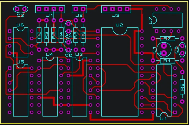
1. Group Components by Function
Start by grouping components based on their function. For example, place all components related to power supply circuits in one area and digital signal components in another. This reduces the length of traces between related parts, minimizing signal delays and potential interference. Functional grouping also makes troubleshooting easier during testing and maintenance.
2. Prioritize Critical Components
Identify critical components like microcontrollers, oscillators, and high-speed transceivers, and place them first. These components often have strict placement requirements due to their sensitivity to noise or timing constraints. Positioning them early ensures you can optimize their connections and meet design specifications.
3. Minimize Trace Lengths
Shorter traces reduce signal propagation delays and lower the risk of noise pickup. Place components that frequently communicate with each other close together to keep traces as short as possible. For instance, in a high-speed design, placing a memory chip near a processor can reduce trace lengths and improve data transfer rates.
4. Consider Thermal Management
Heat-generating components like power regulators and high-current transistors should be placed away from heat-sensitive parts. Ensure there’s enough space for heat dissipation, and consider proximity to heat sinks or ventilation if needed. Proper thermal placement prevents overheating and extends the lifespan of your board.
Placement Strategies for Noise Reduction
Noise is a major concern in PCB design, as it can degrade signal integrity and cause malfunctions. Implementing noise reduction strategies during component placement can significantly improve performance. Here are some actionable tips to minimize noise in your designs.
1. Separate Analog and Digital Sections
Analog and digital circuits have different noise characteristics. Digital circuits often produce high-frequency noise that can interfere with sensitive analog signals. To prevent this, physically separate analog and digital sections on your PCB. Use distinct ground planes for each section, connected at a single point to avoid ground loops.
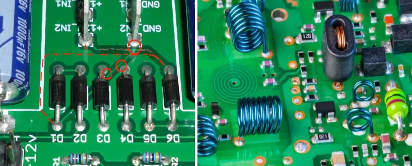
2. Place Decoupling Capacitors Close to ICs
Decoupling capacitors are essential for filtering noise in power supply lines. Place these capacitors as close as possible to the power pins of integrated circuits (ICs). A general rule is to keep the capacitor within 0.1 inches (2.54 mm) of the IC pin to minimize inductance in the connection. For high-speed designs, use multiple capacitors with values like 0.1 μF and 1 μF to cover a range of frequencies.
3. Avoid Long, Parallel Traces
Long, parallel traces can act as antennas, picking up or radiating electromagnetic interference (EMI). When placing components, arrange them to avoid long parallel routing paths. If parallel traces are unavoidable, space them at least 3 times the trace width apart to reduce crosstalk.
High-Speed Component Placement Techniques
High-speed PCB designs, where signal frequencies exceed 100 MHz or rise times are below 1 ns, require extra care during component placement. Signal integrity issues like reflections, crosstalk, and timing errors become more pronounced at these speeds. Let’s explore strategies tailored for high-speed applications.
1. Optimize Signal Path Lengths
In high-speed designs, signal timing is critical. Place components to ensure signal paths are as short and direct as possible. For differential pairs, such as those used in USB or HDMI interfaces, match the lengths of the positive and negative traces to within 5 mils (0.127 mm) to prevent skew and maintain signal integrity.
2. Place Clock Components Strategically
Clock signals are highly sensitive to noise and interference. Position clock sources, like crystal oscillators, close to the devices they drive. Keep clock traces short and avoid routing them near high-noise areas, such as power switching circuits. Surround clock traces with a ground plane to shield them from interference.
3. Use Controlled Impedance Layouts
High-speed signals require controlled impedance to prevent reflections. During placement, ensure components are arranged to support consistent trace widths and spacing. For example, a 50-ohm impedance trace, common in RF designs, should maintain a uniform width and be routed over a continuous ground plane. Placement should facilitate this by avoiding sharp bends or unnecessary vias.
Component Orientation Tips for Better Performance
The orientation of components on a PCB can influence signal flow, noise levels, and ease of manufacturing. While often overlooked, proper orientation is a simple yet effective way to enhance your design.
1. Align Components for Signal Flow
Orient components so that signal flow follows a logical path, reducing the need for complex routing. For example, in a data processing circuit, align components like ADCs, processors, and memory chips in the direction of data flow. This minimizes trace crossings and simplifies the layout.
2. Standardize Orientation for Manufacturing
For automated assembly, orient similar components (like resistors or capacitors) in the same direction. This reduces the risk of placement errors during manufacturing and speeds up the assembly process. Check design for manufacturability (DFM) guidelines to ensure compliance with assembly requirements.
3. Rotate Components to Avoid Interference
In dense layouts, rotating components by 45 or 90 degrees can help avoid interference between traces or neighboring parts. For instance, rotating a capacitor by 90 degrees near an IC might provide a clearer path for routing power traces, reducing noise pickup.
Advanced Strategies for Complex Designs
For complex PCBs with high component density or mixed-signal systems, additional strategies can further optimize performance and reduce noise.
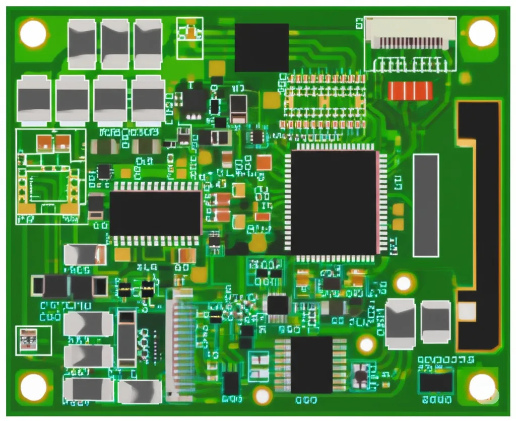
1. Use Multi-Layer Boards for Separation
In multi-layer PCBs, dedicate specific layers to power and ground planes. This provides shielding between signal layers, reducing EMI. Place high-speed components on outer layers for easier access to ground planes, and route sensitive signals on inner layers for added protection.
2. Implement Star Grounding for Mixed-Signal Designs
In mixed-signal designs, use a star grounding technique where all ground connections meet at a single point. This prevents ground loops, which can introduce noise into analog circuits. During placement, ensure components are positioned to facilitate this grounding approach.
3. Plan for Testability
Place test points and debug headers in accessible locations during the initial layout. This ensures you can easily test and troubleshoot the board without disrupting critical components. For high-speed designs, consider adding test pads near critical signals for oscilloscope measurements.
Common Mistakes to Avoid in PCB Component Placement
Even experienced designers can make placement errors that lead to performance issues. Here are some common mistakes to watch out for:
- Ignoring Ground Planes: Failing to include a continuous ground plane can increase noise and EMI. Always place components with grounding in mind.
- Overcrowding Components: Packing components too tightly can lead to thermal issues and make routing difficult. Leave adequate spacing, especially around high-power parts.
- Neglecting Via Placement: Excessive or poorly placed vias can disrupt signal integrity in high-speed designs. Position components to minimize via usage in critical paths.
Tools and Resources for Effective Placement
Modern PCB design software offers powerful features to assist with component placement. Use auto-placement tools to get a rough layout, then manually refine it based on the strategies discussed. Simulation tools can also help predict noise and signal integrity issues before manufacturing, saving time and cost.
Additionally, refer to manufacturer datasheets for specific placement recommendations, especially for high-speed or sensitive components. These documents often provide detailed guidelines on decoupling, grounding, and orientation.
Conclusion: Building Better PCBs with Strategic Placement
Mastering PCB component placement is a critical skill for any electronics designer. By following the strategies outlined in this guide, such as grouping components by function, minimizing trace lengths, and optimizing for high-speed signals, you can maximize performance and minimize noise in your designs. Thoughtful placement not only improves signal integrity but also enhances thermal management and manufacturability.
Whether you're designing a simple circuit or a complex high-speed system, prioritize placement from the start. With careful planning and attention to detail, you can create reliable, efficient PCBs that meet the demands of modern electronics. Start applying these placement strategies in your next project to see the difference they make!


