ALLPCB


Introduction
Proper clearance between traces on a printed circuit board (PCB) is essential for ensuring electrical reliability and safety, particularly in designs handling elevated voltage levels. Insufficient spacing can lead to arcing, dielectric breakdown, or short circuits, compromising the entire system's performance. This guide provides electric engineers with a structured approach to calculating trace clearance, drawing on established industry standards like IPC-2221B. Engineers often rely on trace clearance calculators integrated into PCB design software to streamline this process while accounting for voltage levels and environmental conditions. By understanding the underlying principles, you can optimize layouts for high-voltage applications without overdesigning. This article covers definitions, key factors, calculation methods, and best practices to help you achieve compliant and robust PCB designs.
What Is Trace Clearance and Why Does It Matter?
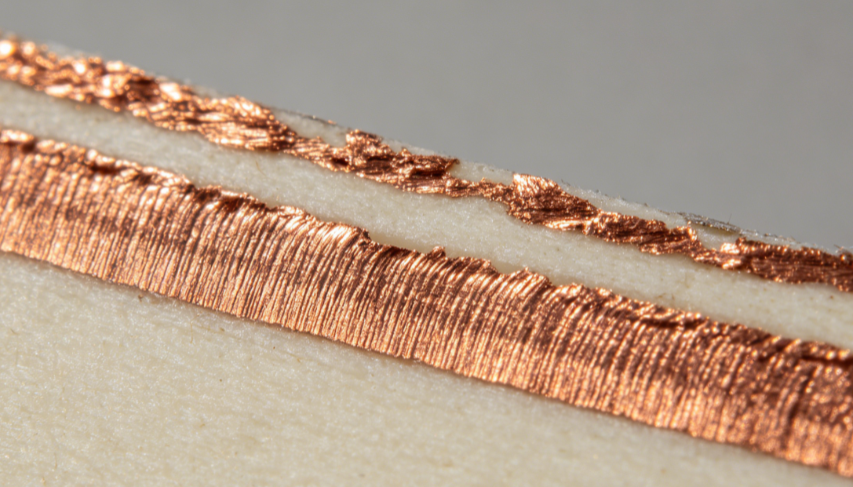
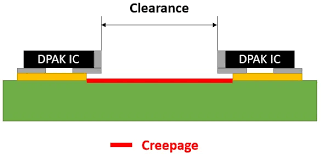
Trace clearance refers to the shortest straight-line distance through air between two conductive elements, such as traces, pads, or vias on a PCB. It differs from creepage, which measures the path along the board surface between conductors, as clearance focuses purely on the air gap to prevent partial discharges or flashover. In PCB design, maintaining adequate clearance is critical to avoid electrical breakdown under operating conditions. For instance, at higher voltage levels, the electric field strength across a small gap intensifies, increasing arcing risk.
The relevance of trace clearance extends to safety certifications, product reliability, and regulatory compliance in applications ranging from power supplies to industrial controls. Poor clearance can result in field failures, especially in harsh environmental conditions like high altitude or humidity, where air insulation properties degrade. Industry standards such as IPC-2221B categorize clearance requirements based on conductor location and voltage to guide designers systematically. Neglecting these can lead to costly redesigns or safety hazards, making precise calculation a cornerstone of professional PCB engineering.
Key Technical Principles Governing Trace Clearance
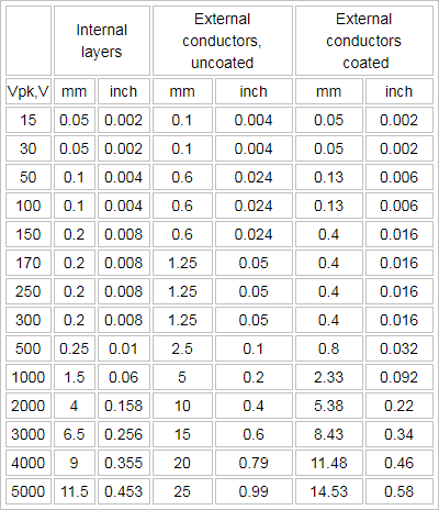
The primary mechanism behind trace clearance requirements is the dielectric strength of air, which limits how much voltage a given gap can withstand before ionization occurs. IPC-2221B outlines minimum electrical conductor spacings in Table 6-1, differentiating between internal layers (B1) and external conductors, with adjustments for coatings and altitude. For example, internal conductors (B1) require only 0.05 mm spacing for voltages up to 30 V, while external uncoated traces (B2) at sea level to 3050 m demand 0.6 mm for 31-100 V ranges. These values ensure the electric field remains below air's breakdown threshold, typically around 3 kV/mm under standard conditions.
Voltage levels play a pivotal role, with standards specifying peak AC or DC values between conductors. Environmental conditions further modulate requirements: at altitudes above 3050 m (B3 category), clearances increase due to lower air density reducing insulation effectiveness. Pollution degrees and humidity primarily impact creepage but indirectly influence clearance in contaminated setups by promoting tracking. Conductor coatings, like polymer (B4) or conformal (A5), allow reduced spacings by enhancing surface insulation.
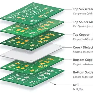
Layer stackup also affects clearance: internal planes benefit from embedded dielectrics, permitting tighter spacings than exposed external traces vulnerable to dust or moisture. For voltages exceeding 500 V, IPC-2221B instructs adding incremental values per volt to the 500 V baseline, ensuring scalability for high-power designs. These principles form the foundation for accurate calculations in PCB design software.
Factors Influencing Trace Clearance Calculations
Several interrelated factors determine the required trace clearance, starting with the maximum expected voltage between any two conductors. Engineers must consider both steady-state DC and transient AC peaks, often derived from circuit simulations or specifications. PCB design software automates this by applying IPC-based rules, but manual verification remains essential for edge cases.
Environmental conditions significantly alter baseline values. Altitude reduces atmospheric pressure, weakening air's dielectric properties and necessitating larger gaps for B3 categories. Operating temperature indirectly affects clearance through material expansion, though standards prioritize voltage and location. Pollution levels, while more critical for creepage, can deposit conductive particles that bridge air gaps over time.
Conductor attributes refine the calculation: internal traces (B1) tolerate smaller clearances due to laminate encapsulation, whereas external uncoated ones (B2) require conservatism. Coatings mitigate this; polymer-coated external traces (B4) halve some spacings compared to uncoated. Fabric width and routing topology also interplay, as wider traces intensify fields at edges.
Board material's comparative tracking index (CTI) influences creepage more, but high-CTI laminates support overall spacing strategies. Finally, system-level factors like overvoltage categories from IEC 60664-1 provide context for impulse withstand, aligning PCB clearance with end-equipment needs.
Practical Steps for Calculating Trace Clearance
To calculate clearance systematically, begin by identifying the highest voltage differential across traces using schematic analysis. Determine conductor classification: internal, external uncoated, coated, or component leads. Consult IPC-2221B Table 6-1 for the corresponding minimum spacing; for instance, external uncoated traces (B2) at 101-250 V need 1.25 mm.
Next, integrate environmental conditions. For altitudes over 3050 m, scale up B2 values per standard modifiers. Leverage a trace clearance calculator in your PCB design software, inputting voltage levels, layer type, and conditions to generate rules. Verify via design rule checks (DRC), ensuring no violations post-routing.
For complex multilayer boards, apply net-class rules differentiating high-voltage nets. If spacings prove challenging, consider conformal coating to shift to A5/B4 categories, recalculating accordingly. Document assumptions, such as peak voltage margins, for fab handover.
Best Practices and Troubleshooting Common Issues
Adopt a hierarchical rule system in PCB design software: global minimums for low-voltage signals (e.g., 0.1 mm), escalating for power nets. Always exceed minimums where space allows to buffer manufacturing tolerances. Pair clearance with creepage rules, as surface paths often govern external layouts.
Troubleshoot by reviewing DRC violations: trace too close to planes? Reroute or add slots. High-voltage arcing suspected in prototypes? Measure actual gaps with calipers and correlate to voltage logs. Environmental testing reveals issues like altitude derating; simulate via software or altitude chambers.
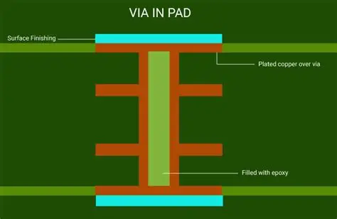
Incorporate vias and pads thoughtfully, as they demand equivalent clearances. For dense designs, use buried vias for high-voltage routing. Regularly update rules against latest standards interpretations.
Conclusion
Calculating clearance between traces demands a methodical evaluation of voltage levels, conductor types, and environmental conditions, anchored in IPC-2221B guidelines. By employing trace clearance calculators within PCB design software and adhering to structured steps, electric engineers can prevent failures and ensure compliance. Prioritizing these practices yields reliable, high-performance PCBs suited to demanding applications. Master these principles to elevate your design expertise.
FAQs
Q1: How does a trace clearance calculator work in PCB design software?
A1: Trace clearance calculators in PCB design software automate IPC-2221B Table 6-1 lookups, inputting voltage levels, layer types, and environmental conditions to output minimum spacings. Select conductor categories like B1 for internal or B2 for external uncoated, then apply net-specific rules. This ensures DRC compliance, reducing manual errors in high-voltage layouts. Verify outputs against standards for accuracy.
Q2: What role do IPC standards play in determining PCB trace clearance?
A2: IPC standards, particularly IPC-2221B, define minimum conductor spacings via tables categorized by voltage ranges and locations. They distinguish internal from external traces, accounting for coatings to prevent breakdown. Engineers reference these for reliable designs across voltage levels. Compliance supports safety and manufacturability.
Q3: How do environmental conditions affect trace clearance requirements?
A3: Environmental conditions like altitude above 3050 m increase clearances for external traces (B3 category) due to reduced air density. Humidity and pollution indirectly impact via creepage but warrant conservative air gaps. Use PCB design software to derate values, ensuring robustness in varied deployments. Standards like IPC-2221B provide explicit modifiers.
Q4: Why separate clearance calculations for internal versus external traces?
A4: Internal traces (B1) enjoy laminate protection, allowing tighter spacings like 0.05 mm up to 30 V per IPC-2221B. External uncoated traces (B2) face direct exposure, requiring larger gaps such as 0.6 mm for 31-50 V to resist arcing. This differentiation optimizes density while maintaining insulation integrity.
References
IPC-2221B — Generic Standard on Printed Board Design. IPC
IEC 60664-1 — Insulation Coordination for Equipment within Low-Voltage Systems. IEC