 ALLPCB


Introduction
Medical devices continue to evolve toward smaller, more efficient designs that enhance patient comfort and functionality. High-density interconnect (HDI) PCBs play a pivotal role in this shift, enabling miniaturization medical electronics through advanced features like microvias and finer trace geometries. These next-generation medical PCBs support applications from implantable devices to portable diagnostics, where space constraints demand higher component density without compromising reliability. Engineers must understand these trends to design boards that meet stringent performance requirements in healthcare environments. As medical electronics advance, HDI PCB medical devices emerge as essential for integrating complex circuitry into compact form factors. This article explores key developments, technical principles, and practical strategies for implementing advanced PCB technology medical solutions.
What Are HDI PCBs and Why They Matter in Medical Devices
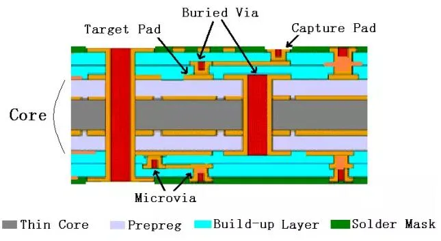
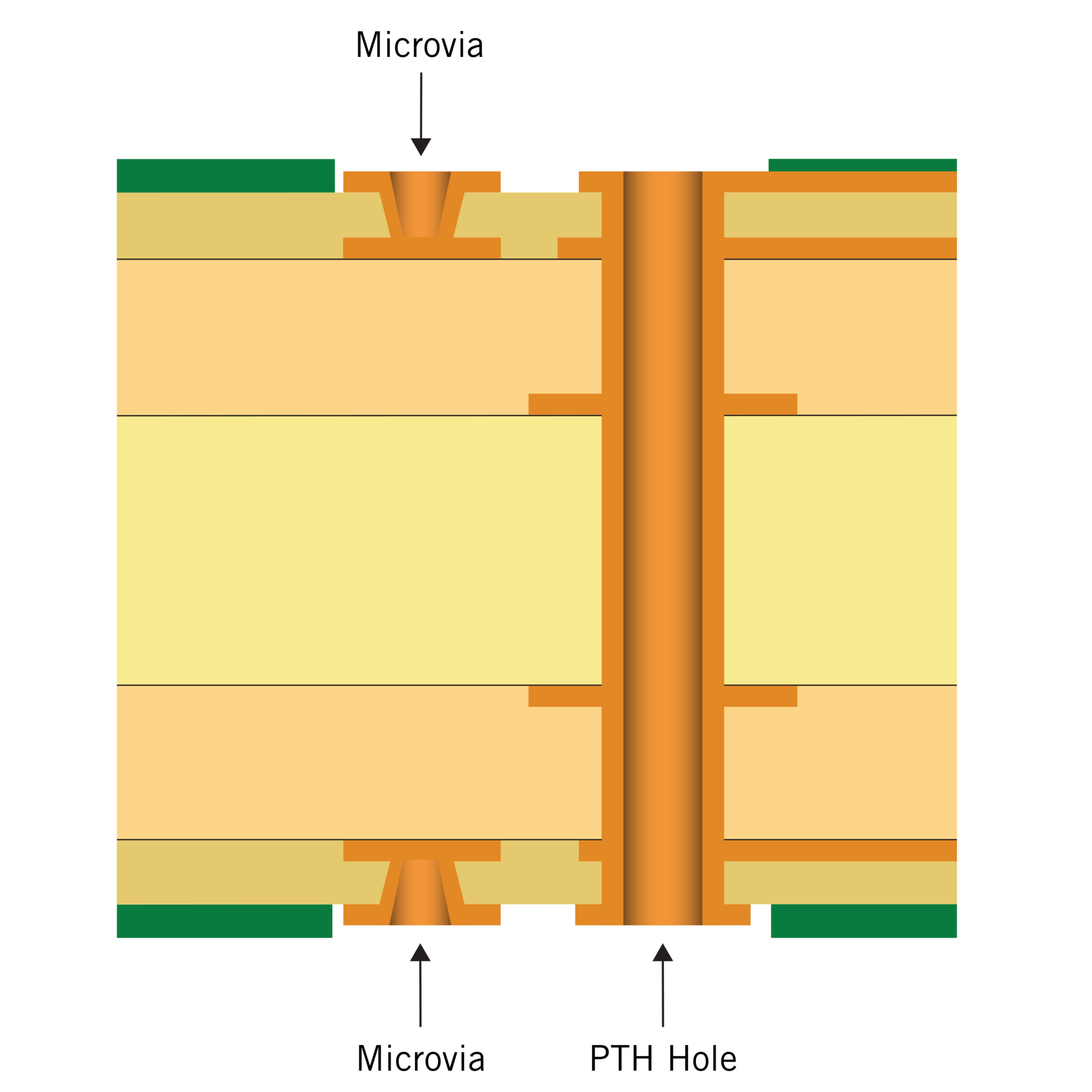
HDI PCBs differ from conventional boards by incorporating microvias, blind vias, and buried vias to achieve greater wiring density per unit area. Microvias medical PCB typically have diameters of 150 microns or less, allowing connections between closely spaced layers without penetrating the entire stackup. In medical contexts, these features enable miniaturization medical electronics, such as in pacemakers or endoscopes, where every millimeter counts for invasiveness and wearability. The relevance stems from the need for high-speed signal transmission and power delivery in dense layouts, critical for real-time monitoring and therapeutic functions. HDI structures reduce signal path lengths, minimizing latency and electromagnetic interference in sensitive diagnostics. Compliance with standards like IPC-2226 ensures these designs maintain integrity under operational stresses.
Technical Principles Driving Miniaturization in Medical PCBs
Miniaturization in medical PCBs relies on laser-drilled microvias that provide precise interlayer connections with minimal footprint. Stacked microvias connect multiple layers sequentially, while staggered configurations offset vias to improve reliability by distributing stress. Advanced PCB technology medical incorporates these with finer line widths and spaces, often below 50 microns, to pack more components into limited areas. Material selection focuses on low coefficient of thermal expansion (CTE) dielectrics to prevent warpage during assembly reflow processes. Signal integrity benefits from shorter via stubs, reducing impedance discontinuities at high frequencies common in imaging devices. Thermal management becomes crucial as density increases heat generation, necessitating embedded heat spreaders or vias-in-pad designs.
The evolution toward ultra-HDI pushes microvia diameters under 75 microns, enabling even tighter pitches for ball grid arrays (BGAs) in next-generation medical PCB assemblies. Build-up processes layer thin dielectrics and copper foils sequentially, forming complex netlists with high fanout. Engineers must model via transitions using field solvers to predict crosstalk and loss, especially in RF-enabled implants. Power integrity challenges arise from thin cores, requiring careful plane splitting and decoupling capacitor placement near ICs. These principles collectively allow HDI PCB medical devices to support multi-gigabit data rates in compact housings.
Key Trends Shaping Microvias Medical PCB Development
Current trends in microvias medical PCB emphasize reliability enhancements through filled and plated structures that withstand thermal cycling. Laser direct imaging (LDI) enables sub-30 micron features, aligning with demands for 0.3 mm pitch BGAs in handheld diagnostics. Hybrid rigid-flex HDI combines the density of rigid sections with flexibility for wearables, reducing overall device volume. Integration of embedded passives and actives directly into the board further drives miniaturization medical electronics by eliminating surface-mount footprints. Sequential lamination builds allow any-layer vias, connecting arbitrary layers without through-hole interference. These advancements position advanced PCB technology medical at the forefront of implantable neurostimulators and lab-on-chip systems.
Sustainability influences material choices, favoring lead-free finishes and recyclable resins without sacrificing performance. High-frequency laminates with low dielectric constants support 5G-enabled telemedicine devices. Yield optimization through process controls addresses defect risks in stacked via chains. Overall, these trends forecast continued density doubling every few years, guided by IPC-6012DS qualification requirements for microvia integrity.
Challenges in Implementing HDI for Next-Generation Medical PCBs
Dense HDI layouts introduce electromigration risks at high currents, particularly in thin traces serving power-hungry sensors. Via reliability under shock and vibration demands aspect ratios below 1:1, as steeper drills increase voiding during plating. Thermal mismatch between copper and dielectrics causes cracking in stacked microvias during repeated sterilization cycles. Signal skew in asymmetric stackups requires length matching and backdrilling for controlled impedance. Manufacturing tolerances tighten to microns, challenging drill registration and photoresist adhesion on sequential layers. Medical applications amplify these issues, as failures could impact patient safety, necessitating Class 3A compliance per relevant IPC guidelines.
Resolving these involves simulation-driven design, verifying via chain continuity through flying probe testing. Plating uniformity across panels prevents hotspots that degrade long-term performance. Cost escalates with layer count, but yields improve via design-for-manufacturability (DFM) rules like teardrop pads.
Best Practices for Designing and Fabricating HDI PCB Medical Devices
Start with stackup planning per IPC-2226, selecting via configurations based on layer count and escape requirements. Staggered vias suit moderate densities, while stacked excel for ultra-fine pitch but demand filled plating. Maintain microvia aspect ratios under 0.8:1 and limit stacking to three levels initially to ensure fill completeness. Use laser-drillable dielectrics with consistent ablation rates for clean holes. Simulate power delivery networks early to avoid ground bounce in dense IC arrays. For assembly, incorporate fiducials and panelization optimized for pick-and-place accuracy.
In fabrication, sequential build-up with photo-defined patterning minimizes undercuts on fine features. Post-lamination planarization via chemical-mechanical polish ensures flatness for subsequent layers. Reliability testing includes thermal shock, as outlined in IPC standards, to validate microvia shear strength. Documentation should detail build sequence and material callouts for traceability. These practices enable robust HDI PCB medical devices ready for regulatory scrutiny.
Future Outlook for Advanced PCB Technology Medical
Emerging techniques like panel-level packaging integrate HDI with fan-out redistribution layers for heterogeneous integration. Photonics integration via polymer waveguides promises optical signaling in implants, bypassing electrical limits. AI-optimized routing automates via placement for optimal density. Quantum dot sensors paired with HDI enable molecular-level diagnostics in pill-sized devices. Biocompatible coatings protect boards in vivo applications. These horizons redefine miniaturization medical electronics, blending PCBs with system-in-package paradigms.
Conclusion
HDI PCBs represent the cornerstone of future medical electronics, with microvias and high-density features enabling unprecedented miniaturization. Engineers leveraging standards like IPC-2226 and best practices in design and fabrication can overcome challenges in reliability and performance. Trends toward ultra-fine features and hybrid structures promise transformative devices for healthcare. Prioritizing signal integrity, thermal control, and DFM ensures next-generation medical PCB success. As demands grow, HDI PCB medical devices will drive innovations in patient care and diagnostics.
FAQs
Q1: What are HDI PCB medical devices, and how do they support miniaturization?
A1: HDI PCB medical devices use microvias, blind, and buried vias to achieve high interconnect density in compact formats. This allows miniaturization medical electronics by reducing board size while accommodating more components for functions like real-time monitoring. Designs follow IPC guidelines for reliability under medical stresses. Engineers benefit from shorter signal paths that enhance speed and reduce power consumption. Overall, they enable wearable and implantable tech with superior performance.
Q2: Why are microvias essential in medical PCBs?
A2: Microvias medical PCB provide precise, small-diameter connections (under 150 microns) that maximize routing density without full stackup penetration. They support advanced PCB technology medical by enabling fine-pitch BGAs and multilayer nets in space-limited devices. Challenges like fill reliability are addressed through plating and aspect ratio controls. In practice, they improve signal integrity for high-frequency medical signals. This makes them indispensable for next-generation medical PCB trends.
Q3: What challenges arise with miniaturization medical electronics in HDI designs?
A3: Miniaturization medical electronics via HDI introduces thermal management issues from dense heat sources and via cracking risks in stacked structures. Signal integrity demands impedance control amid short paths and crosstalk. Manufacturing requires tight tolerances for laser drilling and plating uniformity. Best practices include simulation and IPC-2226 compliance to mitigate failures. Reliability testing ensures suitability for critical applications.
Q4: How can engineers implement best practices for next-generation medical PCB?
A4: For next-generation medical PCB, start with stackup optimization using staggered microvias for balanced stress. Adhere to IPC standards for qualification, limiting via chains and using filled structures. Simulate SI/PI early and incorporate DFM for yield. Select low-CTE materials to combat warpage. These steps deliver robust HDI PCB medical devices ready for assembly and deployment.


