 ALLPCB


Introduction
Wearable technology continues to transform personal health monitoring, fitness tracking, and everyday computing with devices that conform to the human body. High-density interconnect (HDI) PCBs play a pivotal role in enabling these compact, high-performance systems by packing more functionality into smaller spaces. HDI PCB wearable devices demand not just density but also flexibility to withstand bending, twisting, and constant motion. Engineers designing for smartwatches, fitness bands, and medical patches must navigate challenges like signal integrity and mechanical reliability. This article explores flexible HDI PCB design principles and their specific applications in HDI PCB smartwatches and HDI PCB medical wearables. By understanding these technologies, electric engineers can optimize designs for real-world durability and performance.
What Are HDI PCBs and Why Do They Matter in Wearables?
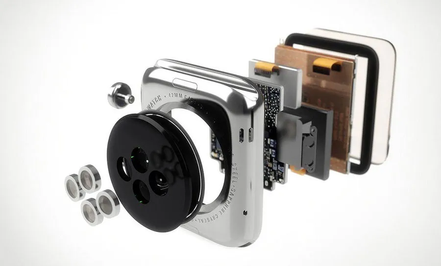
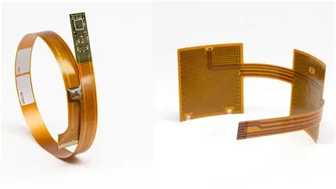
HDI PCBs feature finer lines, smaller vias, and more layers compared to standard boards, achieved through microvias, blind vias, and buried vias. These structures allow for higher component density, essential for wearable devices where space is at a premium. In wearables, HDI enables integration of sensors, processors, and batteries into ultrathin profiles under 1 mm thick. Flexible HDI PCB design extends this by incorporating polyimide substrates that bend without fracturing, unlike rigid FR-4. This combination addresses the need for devices that wrap around wrists or conform to skin for continuous monitoring.
The relevance stems from market demands for lighter, more comfortable wearables. Traditional PCBs limit miniaturization, leading to bulkier designs that users reject. HDI PCB wearable devices reduce size by up to 50% while supporting high-speed signals for Bluetooth and GPS. For electric engineers, mastering HDI means balancing electrical performance with mechanical stress from daily wear. Standards like IPC-2226 guide these designs, ensuring via reliability under flex cycles.
Technical Principles of HDI in Flexible Wearable Applications
HDI PCBs build density through sequential lamination, where laser-drilled microvias connect layers without penetrating the entire stack. Type 1 HDI (1+n+1) uses a single microvia layer on both sides of a core, ideal for basic smartwatches. Advanced types like 2+n+2 stack multiple microvia layers, suiting HDI PCB medical wearables with ECG sensors and accelerometers. Flexible variants employ adhesive-less laminates to prevent delamination during bending radii as tight as 1 mm.
Signal integrity relies on controlled impedance traces, often 50 microns wide, with via-in-pad for shortest paths. Materials like liquid crystal polymer (LCP) or polyimide offer low dielectric constants and high bend endurance over 100,000 cycles. Thermal management poses challenges, as wearables generate heat from processors during data processing. Engineers must model via thermal resistance to avoid hotspots that degrade adhesives.
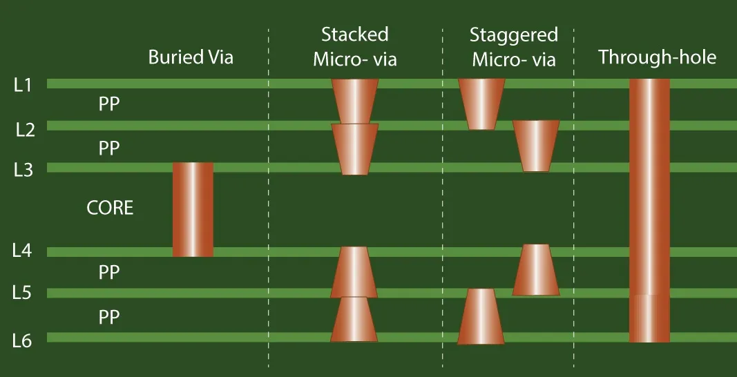
Manufacturing involves precise laser ablation for vias under 75 microns, followed by electroplating for fill. Fill styles like staggered or filled vias per IPC-2226 prevent cracks in flex areas. Reliability testing simulates wear, including cyclic bending and vibration per industry protocols. These principles ensure HDI PCB smartwatches maintain Wi-Fi connectivity without intermittent failures.
Flexible HDI PCB Design: Key Engineering Considerations
Flexible HDI PCB design requires tailoring stackups to application stresses, starting with substrate selection for CTE matching. Polyimide films with copper foils rolled-annealed for ductility handle dynamic flex better than electrodeposited copper. Design rules specify minimum bend radius as 10 times substrate thickness to avoid trace cracking. Engineers use teardrop pads at vias to distribute stress and reduce failures in high-flex zones.
Component placement prioritizes rigid sections for BGAs and flex tails for sensors, forming rigid-flex hybrids. This hybrid approach suits HDI PCB wearable devices like fitness trackers, where rigid islands host ICs and flex bridges connect to straps. Signal routing avoids 90-degree bends, using 45-degree angles for better fatigue resistance. Simulation tools verify strain during 90-degree folds common in wristbands.
Assembly challenges include warpage from thin cores, mitigated by carrier panels during lamination. Solder joints must withstand shear from motion, following J-STD-001 for Class 3 reliability. Troubleshooting common issues like microvia opens involves X-ray inspection post-lamination. Electric engineers iterating prototypes focus on these to achieve yields over 95% in production.
Best Practices for Implementing HDI PCBs in Wearables
Start with DFM reviews incorporating IPC-6012 qualification criteria for microvia integrity. Define via capture and target pad sizes at 75 microns minimum to ensure laser drill accuracy. Layer sequencing optimizes for shortest vias first, reducing aspect ratios under 1:1. For HDI PCB medical wearables, incorporate filled vias in sensor areas to enable fine-pitch BGAs down to 0.3 mm.
Material qualification tests flex endurance and humidity resistance, critical for sweat-exposed devices. Use coverlays with laser-cut openings for components, maintaining IP67 sealing. Power distribution employs embedded passives to shrink footprints further. Validation includes thermal cycling from -40°C to 85°C to mimic body temperatures.
Production scaling demands panel-level processing for cost efficiency, with fiducials for alignment. Troubleshooting delamination traces back to adhesive voids, resolved by vacuum lamination. Engineers document stackup deviations early to align with fabricator capabilities. These practices ensure robust HDI PCB smartwatches ready for volume assembly.
Troubleshooting Common Challenges in Flexible HDI Wearables
Flex cracking often appears after 50,000 cycles, linked to trace etch control. Inspect with cross-polarization microscopy to detect microcracks early. Signal crosstalk in dense routing requires ground stitching vias every 0.5 mm. For HDI PCB wearable devices, EMI shielding via grounded flex layers prevents interference with heart rate sensors.
Battery integration strains flex areas; reinforce with wider traces and polyimide stiffeners. Thermal runaway in processors triggers adhesive softening, addressed by via heat sinks. Field failures from moisture ingress demand conformal coatings compatible with flex. Systematic root cause analysis using failure mode effects keeps designs evolving.
Conclusion
HDI PCBs redefine wearable technology by merging high density with flexibility, enabling sleeker HDI PCB smartwatches and reliable HDI PCB medical wearables. Engineers leverage microvias, advanced materials, and standards like IPC-2226 for designs that endure real-world use. Flexible HDI PCB design best practices focus on stress distribution, material matching, and rigorous testing. As wearables integrate more AI and sensors, HDI will drive further innovation. Prioritizing these principles ensures performance, comfort, and longevity in next-generation devices.
FAQs
Q1: What makes HDI PCB wearable devices suitable for smartwatches?
A1: HDI PCB wearable devices excel in smartwatches due to microvias and fine lines that fit processors, displays, and sensors into tiny footprints. Flexible HDI PCB design adds bendability for wrist conformity without signal loss. Per IPC-2226, stacked vias maintain integrity under motion. This results in thinner, lighter watches with extended battery life and reliable Bluetooth connectivity. Engineers troubleshoot via reliability to avoid field failures.
Q2: How does flexible HDI PCB design improve medical wearables?
A2: Flexible HDI PCB design in medical wearables allows skin-conformable patches for ECG and glucose monitoring with high-density sensor arrays. It handles 100,000+ bend cycles using polyimide and filled microvias. J-STD-001 assembly ensures robust joints under sweat and strain. Troubleshooting focuses on CTE mismatch to prevent delamination. This enables continuous, comfortable vital sign tracking.
Q3: What are key challenges in HDI PCB smartwatches?
A3: HDI PCB smartwatches face thermal management and flex fatigue from daily wrist motion. Microvia cracking occurs if bend radii exceed design limits. Signal integrity demands controlled impedance routing. Best practices include IPC-6012 testing for qualification. Electric engineers resolve these through iterative simulation and X-ray inspection for production-ready boards.
Q4: Why choose HDI for flexible wearable applications?
A4: HDI integrates high-speed signals and components in flex substrates, shrinking HDI PCB wearable devices by 40%. It supports rigid-flex hybrids for mixed rigid ICs and flex sensors. Standards guide via plating for reliability. Troubleshooting EMI ensures clear data transmission. This technology future-proofs wearables for advanced features like AR overlays.


