 ALLPCB


Environmental Footprint of PCB Manufacturing
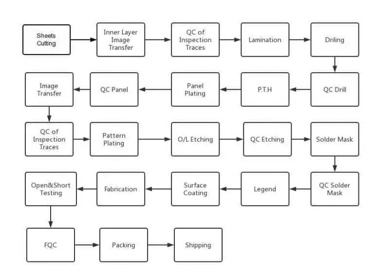
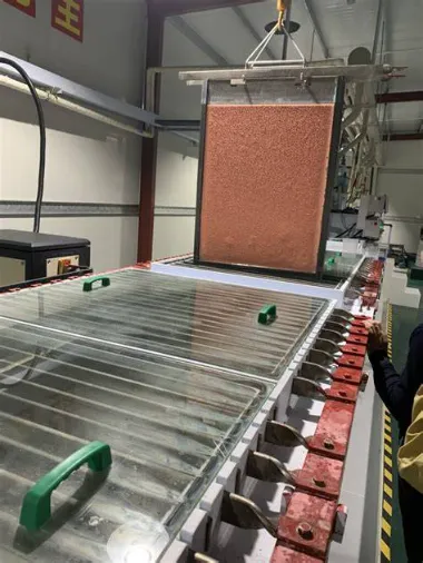
PCB production typically begins with substrate preparation, followed by copper cladding, imaging, etching, drilling, and surface finishing. Each stage consumes electricity and process chemicals, with etching solutions and rinse waters requiring treatment before discharge. Energy use varies with factory scale and process efficiency, but thermal processes such as lamination and solder mask curing add measurable demand. Solid waste includes spent etchants, copper sludge, and offcuts from panelization. Compliance with established quality and process standards helps facilities track and reduce these outputs systematically.
Factory-driven monitoring programs often align with ISO 14001 environmental management principles to quantify resource consumption and emissions. Such frameworks encourage systematic recording of water, energy, and chemical usage across production lines. Engineers reviewing supplier capabilities frequently request data on waste treatment effectiveness and recycling rates for metals recovered during processing. These practices support incremental improvements without altering core board functionality.
Material Choices and Their Lifecycle Implications
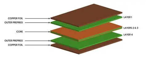
Conventional substrates rely on glass-reinforced epoxy resins that deliver reliable dielectric performance and dimensional stability under IPC-6012E qualification requirements. These materials originate from petroleum-derived resins and mined glass fibers, creating upstream extraction impacts. End-of-life options remain limited because thermoset resins resist easy separation and reprocessing. Lifecycle assessments therefore examine raw material sourcing, manufacturing energy, use-phase durability, and disposal pathways to compare alternatives.
Renewable material candidates include bio-based resins derived from plant oils or lignin, and paper or natural fiber reinforcements. These options can reduce fossil carbon content in the substrate. However, engineers must verify that any substitution maintains thermal, mechanical, and electrical properties required by the application. Standards such as those in the IPC series provide test methods and acceptance criteria that new materials must satisfy before widespread adoption.
Practical Approaches to Lowering Impact
Design teams can reduce board size and layer count where electrical performance permits, directly lowering material volume and processing steps. Panel utilization optimization during layout minimizes scrap generated during routing. Selection of surface finishes with lower heavy-metal content or improved recyclability also contributes to overall profile reduction. Procurement specifications increasingly request supplier declarations on recycled content and waste diversion rates.
Process improvements at the fabrication stage include closed-loop chemical recovery systems and energy-efficient curing equipment. Facilities operating under recognized environmental management systems document these measures and their measured outcomes. Engineers evaluating multiple suppliers compare such data alongside traditional quality metrics to identify lower-impact options that still meet IPC-A-600K acceptability criteria for the finished board.
Challenges in Scaling Renewable Materials
Performance validation remains the primary barrier. Bio-based laminates must demonstrate equivalent glass transition temperature, coefficient of thermal expansion, and moisture resistance to conventional grades under accelerated testing. Variability in natural fiber supply can affect batch consistency, requiring additional incoming inspection protocols. Cost premiums for renewable resins currently limit adoption to applications where environmental criteria carry significant weight in the specification.
Related Reading: Bio-Based Flexible PCBs: A New Frontier in Sustainable Electronics
Supply chain maturity also influences feasibility. Large-scale production of consistent bio-based substrates requires reliable agricultural or forestry feedstocks processed to electronics-grade purity. Until volumes increase, availability and pricing may constrain design choices. Engineers therefore often pursue hybrid approaches, such as specifying boards with standard cores but exploring renewable options for non-critical inner layers or prototypes.
Conclusion
PCB manufacturing carries measurable environmental loads that standards-aligned facilities actively manage through process controls and material stewardship. Renewable substrates offer a pathway to lower fossil resource dependence, yet they require rigorous qualification against existing IPC and related specifications to ensure reliability. Electrical engineers play a central role by incorporating lifecycle considerations into design reviews and supplier evaluations. Continued collaboration between material developers and standards organizations will determine how quickly these alternatives achieve broader acceptance.
FAQs
Q1: How does PCB manufacturing environmental footprint compare across different substrate types?
A1: Conventional glass-epoxy boards and emerging renewable options differ primarily in raw material sourcing and end-of-life behavior. Lifecycle assessments examine extraction, processing energy, and disposal routes. Facilities following ISO 14001 practices can supply comparative data to support engineering decisions.
Q2: What role does renewable PCB materials lifecycle assessment play in supplier selection?
A2: Lifecycle assessment provides a structured method to quantify impacts from cradle to grave. Engineers use the results alongside electrical and reliability requirements when qualifying new materials. Standards-based testing ensures any renewable candidate meets the same performance thresholds as established grades.
Q3: Can sustainable PCB production process changes reduce carbon footprint without affecting board quality?
A3: Targeted improvements in energy efficiency, chemical recovery, and panel utilization lower emissions while preserving product integrity. Compliance with IPC-6012E and related specifications confirms that process modifications do not compromise qualification or acceptability criteria.
Q4: What considerations apply to eco-friendly PCB assembly impact during reflow and cleaning?
A4: Assembly steps contribute additional energy and chemical use. Low-temperature solders and optimized reflow profiles can reduce thermal demand. Waste streams from flux residues and cleaning agents require proper handling consistent with overall facility environmental programs.
References
IPC-6012E — Qualification and Performance Specification for Rigid Printed Boards. IPC, 2017
IPC-A-600K — Acceptability of Printed Boards. IPC, 2020
ISO 14001:2015 — Environmental Management Systems. ISO, 2015





