 ALLPCB


Introduction
The electronics industry continues to seek manufacturing methods that reduce environmental impact while maintaining performance standards. Water-based etching PCB processes represent one area of active exploration, particularly in the context of biodegradable printed circuit boards. These approaches aim to minimize or eliminate traditional chemical etchants, aligning with broader goals of chemical-free PCB manufacturing. Engineers and manufacturers evaluate such techniques for their potential to support eco-friendly PCB etching while meeting reliability requirements in demanding applications. The transition involves careful consideration of material compatibility, process control, and end-of-life disposal characteristics.
Why Water-Based Etching Matters in Modern PCB Production
Traditional copper removal in PCB fabrication relies on acidic or alkaline solutions that require specialized handling, neutralization, and disposal protocols. Water-based etching PCB methods explore alternatives that leverage aqueous solutions or electrolytic processes to achieve selective copper dissolution. This shift supports chemical-free PCB manufacturing initiatives by lowering the volume of hazardous byproducts generated during production. For biodegradable PCBs, compatibility with water-soluble or compostable substrates becomes a key factor, enabling designs that break down more readily after use. Industry professionals assess these processes for scalability, consistency of trace definition, and overall process yield in both prototype and volume production environments.
Technical Principles of Water-Based Etching Mechanisms
In water-based etching PCB operations, the removal of unwanted copper occurs through controlled electrochemical reactions or the use of mildly reactive aqueous media rather than aggressive chemical baths. The process typically begins with the application of a resist pattern that protects desired traces, followed by exposure of the board to the etchant medium. Factors such as solution concentration, temperature, agitation, and exposure time influence etch rate and undercut characteristics. For biodegradable substrates, material stability during the etching step must be verified to prevent dimensional changes or degradation prior to component assembly. Process monitoring often includes measurements of copper thickness reduction and surface quality to ensure compliance with performance specifications.
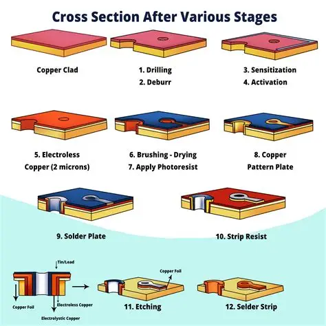
Engineers compare etch uniformity across panels using standardized test coupons. Variations in copper foil thickness or laminate properties can affect outcomes, requiring adjustments in process parameters. In electrolytic variants, current density and electrode configuration play central roles in directing copper removal. These mechanisms differ from conventional immersion etching by offering potential for regeneration or reduced chemical consumption. Validation against established quality criteria helps confirm that finished boards exhibit acceptable trace geometry and surface finish.
Best Practices for Implementing Eco-Friendly PCB Etching
Successful adoption of eco-friendly PCB etching begins with substrate selection that balances electrical performance with environmental objectives. Biodegradable laminates require evaluation for moisture absorption, thermal stability, and compatibility with subsequent assembly steps. Process development includes pilot runs to optimize etchant formulation, dwell times, and post-etch cleaning sequences. Documentation of parameters supports reproducibility and facilitates troubleshooting when trace widths or spacing deviate from design intent.
Quality control integrates visual inspection, electrical testing, and dimensional verification at multiple stages. Adherence to relevant industry standards guides acceptance criteria for finished boards. Teams often implement closed-loop systems for solution management to minimize waste streams. Training for operators emphasizes safe handling practices and proper equipment maintenance to sustain consistent results over extended production periods.
Collaboration between design and manufacturing teams helps identify layout features that facilitate uniform etching, such as balanced copper distribution and appropriate trace spacing. Simulation tools assist in predicting etch behavior before physical trials. Continuous improvement cycles incorporate feedback from yield data and reliability testing to refine the overall workflow.
Considerations for Biodegradable PCB Applications
Biodegradable PCBs introduce additional requirements around end-of-life behavior alongside traditional electrical and mechanical performance metrics. Water-based etching PCB techniques can align with these goals when the etchant medium supports substrate integrity until the final dissolution phase. Material suppliers provide data on degradation rates under specified conditions, which engineers use to validate suitability for target applications. Assembly processes must account for the thermal and chemical sensitivities of these newer laminates.
Reliability testing follows established protocols to confirm that boards withstand operational stresses despite their modified composition. Factors such as via integrity, solder joint formation, and long-term insulation resistance receive particular attention. Documentation of material provenance and process history supports traceability in regulated sectors.
Conclusion
Water-based etching PCB methods offer a pathway toward chemical-free PCB manufacturing that complements the development of biodegradable PCBs. By focusing on aqueous processes and material compatibility, engineers can advance sustainable practices while preserving the precision required for functional electronics. Continued refinement through structured process control and adherence to recognized standards will determine the extent of adoption across various market segments. The integration of these techniques reflects ongoing efforts to balance performance, cost, and environmental responsibility in PCB production.
FAQs
Q1: What defines water-based etching PCB compared with conventional methods?
A1: Water-based etching PCB utilizes aqueous or electrolytic solutions to remove copper instead of strong acidic or alkaline chemistries. This approach supports chemical-free PCB manufacturing objectives by reducing hazardous waste generation. Process parameters require validation to achieve consistent trace quality on both standard and biodegradable substrates.
Q2: How does eco-friendly PCB etching benefit biodegradable board designs?
A2: Eco-friendly PCB etching minimizes chemical residues that could interfere with the degradation profile of biodegradable materials. It enables cleaner separation of copper and components at end of life when paired with water-soluble substrates. Engineers evaluate compatibility during material qualification to ensure overall system performance.
Q3: What standards guide water-based etching PCB process development?
A3: Relevant standards such as IPC-6012E provide qualification criteria for rigid printed boards that apply regardless of etching method. ISO 14001 supports environmental management practices during manufacturing. Teams reference these documents to establish acceptance limits and documentation requirements.
Q4: Are there limitations to chemical-free PCB manufacturing using water-based techniques?
A4: Limitations include potential constraints on etch rate, feature resolution, and compatibility with certain high-reliability applications. Thorough testing confirms that finished boards meet electrical and mechanical specifications. Ongoing research addresses scalability for volume production environments.
References
IPC-6012E — Qualification and Performance Specification for Rigid Printed Boards. IPC, 2017
ISO 14001:2015 — Environmental Management Systems. ISO, 2015
IPC-A-600K — Acceptability of Printed Boards. IPC, 2020


