 ALLPCB


What Is Flying Probe Testing and Why It Matters for Small Businesses
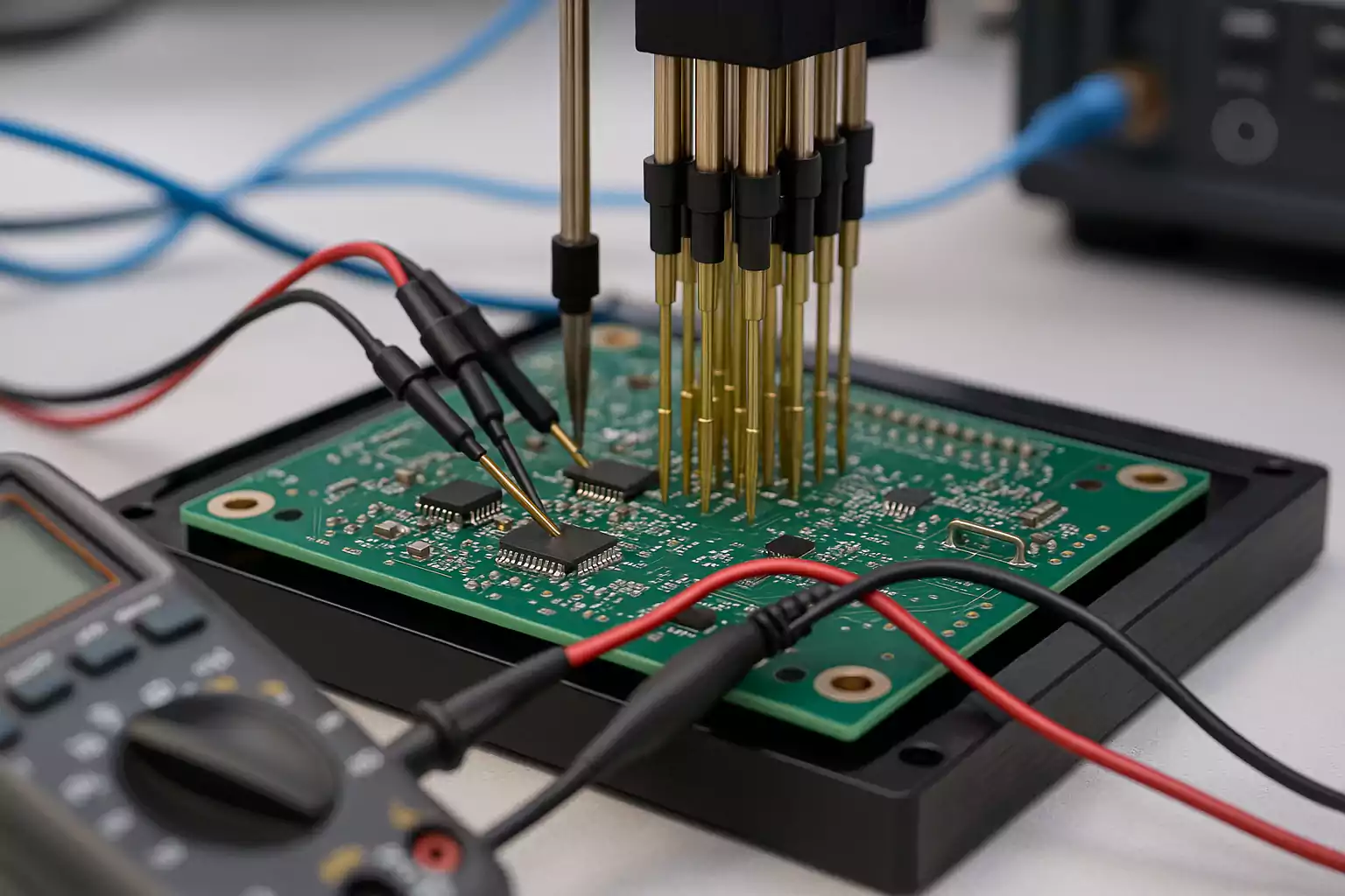
Flying probe testing uses movable probes that contact designated test points on a printed circuit board to perform electrical measurements. Unlike fixture-based methods, it requires no custom hardware for each board design, which reduces upfront investment and setup time. Small businesses benefit because they can test boards of varying designs on the same equipment, supporting flexible production schedules. This capability proves especially useful when volumes remain modest or when designs undergo frequent revisions. The method contributes to small business quality control by identifying opens, shorts, and component value deviations before boards proceed to assembly or end use. It also supports cost-effective testing by minimizing scrap and rework through early detection of issues.
Technical Principles of Flying Probe Testing
The process begins with loading board data that defines netlists and test point locations. Multiple probes, typically four to eight, move independently in the X, Y, and Z axes under computer control to reach the required points. Measurements include continuity, resistance, capacitance, and diode characteristics, which together verify electrical integrity. Probe positioning accuracy and repeatability determine the reliability of results, particularly on boards with fine-pitch features. Test programs can incorporate both in-circuit checks and limited functional verification depending on the equipment configuration. Industry standards such as IPC-A-600K guide the acceptability criteria applied to the measured values.
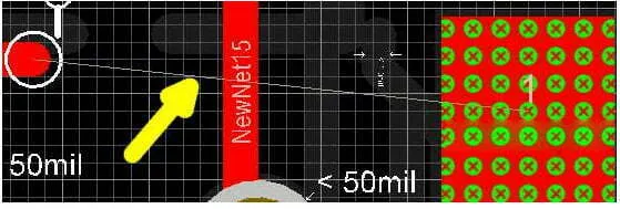
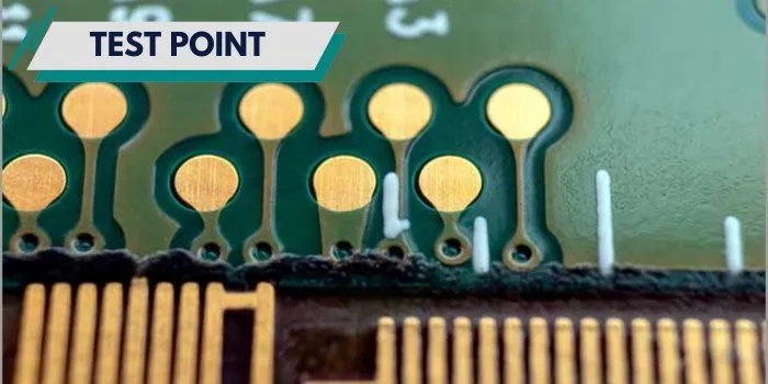
Probe access requires careful consideration during board layout. Test points must remain free of obstructions and sized appropriately for reliable contact. Engineers often incorporate dedicated test pads or vias to improve coverage without compromising signal integrity. The absence of a fixed fixture allows rapid program changes when designs evolve, which suits environments where iteration occurs frequently. Measurement speed depends on the number of tests and board complexity, yet remains acceptable for prototype and low-volume runs common among smaller manufacturers.
Practical Solutions and Best Practices for Implementation
Successful adoption starts with design-for-testability reviews that identify accessible test points early in the layout phase. Engineers should define test coverage goals based on critical nets and component types to balance thoroughness with cycle time. Collaboration between design and test teams helps ensure that probe paths avoid mechanical interference and that sufficient clearance exists around test locations.
Process control includes regular calibration of probe tips and verification of positioning accuracy. Documentation of test programs and results supports traceability required in many quality systems. ISO 9001:2015 principles encourage systematic recording of test parameters and outcomes to facilitate continuous improvement. Organizations typically begin with a pilot program on a representative board to validate program development time and defect detection rates before scaling to additional products.
When test coverage falls short, supplementary methods such as boundary scan or limited functional testing can supplement flying probe results. Data from repeated runs helps refine probe force settings and contact strategies, reducing false failures. Staff training on program generation and result interpretation further improves efficiency and consistency across batches.
Conclusion
Flying probe testing delivers a flexible and economical solution for printed circuit board verification that aligns well with the operational realities of small businesses. Its fixture-free nature lowers barriers to entry while supporting the quality expectations outlined in relevant industry standards. By focusing on design accessibility, program optimization, and process documentation, organizations achieve meaningful defect detection without excessive capital outlay. This approach ultimately strengthens product reliability and supports sustainable growth in competitive markets.
FAQs
Q1: How does flying probe testing for SMEs reduce overall testing expenses compared with traditional methods?
A1: Flying probe testing eliminates the need for custom fixtures that can cost thousands of dollars per board design. Small businesses therefore avoid recurring fixture fabrication and storage costs while retaining the ability to test multiple products on one platform. The method also shortens lead times because program changes require only software updates rather than mechanical rework. These factors combine to make electrical verification more accessible for organizations with limited production volumes.
Q2: What factors determine whether affordable PCB testing with flying probes meets the needs of a specific small business?
A2: Board complexity, required test coverage, and annual volume primarily influence suitability. Designs with adequate test point access and moderate component counts typically achieve good results within acceptable cycle times. Organizations should evaluate sample boards to confirm probe reachability and measurement accuracy before committing to the process. When volumes remain below several thousand units per year, the absence of fixture amortization often favors this approach over bed-of-nails alternatives.
Q3: How can small business quality control teams integrate flying probe testing into existing workflows?
A3: Teams begin by incorporating test point requirements into design reviews and establishing standardized test program templates. Results feed into quality records that support traceability and corrective action processes. Regular equipment maintenance and operator training maintain consistent performance. Integration works best when test data informs both manufacturing adjustments and supplier feedback loops.
Q4: What limitations should engineers consider before adopting cost-effective testing via flying probe methods?
A4: Cycle time increases with the number of test points, which may affect throughput on higher-volume runs. Probe access depends on board layout, so early design involvement is essential. Certain high-frequency or high-power measurements may require complementary techniques. Understanding these constraints allows teams to set realistic expectations and combine methods where necessary.
References
IPC-A-600K — Acceptability of Printed Boards. IPC, 2020
ISO 9001:2015 — Quality Management Systems. ISO, 2015
IPC-6012E — Qualification and Performance Specification for Rigid Printed Boards. IPC, 2017


