 ALLPCB


Introduction
Flexible printed circuit boards (PCBs) have become essential in modern electronics, enabling compact designs in applications like wearables, medical devices, and automotive systems. These boards offer mechanical flexibility and space savings compared to rigid PCBs, but they introduce unique challenges for maintaining signal integrity at high speeds. Flexible PCB signal integrity refers to the ability of signals to propagate without distortion, reflections, or interference, which is critical as data rates increase beyond gigabit per second levels. Poor signal integrity can lead to bit errors, increased power consumption, and system failures, making it a primary concern for engineers designing high-performance flexible circuits.
The dynamic nature of flexible PCBs, including bending and twisting during use, exacerbates issues like impedance variations and crosstalk. Engineers must address these to maximize performance while minimizing noise. This article explores the principles of flexible PCB signal integrity, focusing on impedance control, crosstalk mitigation, and noise reduction strategies. By understanding these elements, designers can achieve reliable operation in demanding environments.
Understanding Signal Integrity in Flexible PCBs
Signal integrity encompasses the preservation of electrical signal quality from transmitter to receiver, ensuring the waveform remains faithful to its original shape. In flexible PCBs, this involves managing transmission line effects, where signals behave as waves rather than lumped elements at high frequencies. Factors such as dielectric materials, trace geometry, and board flexing directly influence signal propagation. Flexible substrates like polyimide have lower dielectric constants than rigid FR-4, affecting wave speed and impedance, but their thin profiles demand precise control to avoid degradation.
Why does signal integrity matter in flexible PCBs? High-speed interfaces like USB 3.0, HDMI, or PCIe require clean signals to prevent eye diagram closure and jitter. In dynamic applications, repeated bending can alter trace dimensions, leading to inconsistent performance over time. Industry standards like IPC-6013 provide qualification requirements for flexible boards, emphasizing electrical testing to verify signal performance. Engineers must prioritize these aspects during design to ensure long-term reliability.
Key Principles of Impedance Control in Flexible PCBs
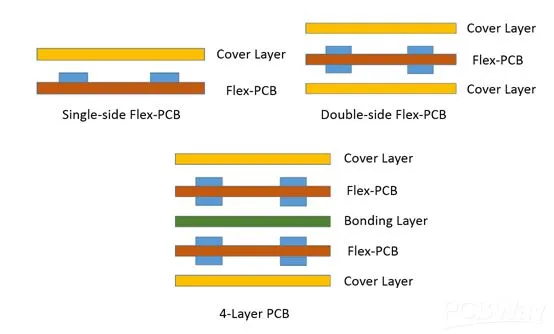
Characteristic impedance in flexible PCBs is determined by the ratio of inductance to capacitance per unit length along a transmission line. Flexible PCB impedance control involves matching this value to the driver's output and receiver's input, typically 50 ohms single-ended or 100 ohms differential. Trace width, dielectric thickness, and copper weight play key roles, with thinner dielectrics in flex circuits requiring narrower traces for the same impedance. Bending introduces variability by compressing or stretching the substrate, which shifts effective dielectric height and thus impedance.
Maintaining consistent impedance minimizes reflections that cause ringing and overshoot. Simulations using field solvers help predict these effects across bend radii and flat regions. Material selection, such as low-loss polyimides, supports better control by reducing signal attenuation. Standards like IPC-2223 guide sectional design for flexible circuitry, recommending practices for impedance stability in production.
Practical implementation starts with stackup optimization, incorporating reference planes adjacent to signal layers. Vias and transitions must preserve impedance, often using back-drilling or tapered designs. Manufacturing tolerances become critical, as variations in copper plating or lamination can detune lines. Testing with time domain reflectometry (TDR) verifies compliance post-fabrication.
Mitigating Crosstalk in Flexible PCBs
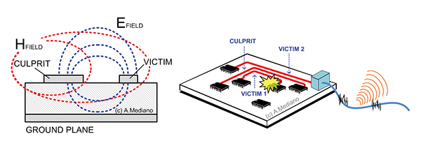
Crosstalk arises from electromagnetic coupling between adjacent traces, manifesting as noise on victim lines from aggressor signals. In flexible PCBs, high trace density and thin dielectrics amplify capacitive and inductive coupling, especially in folded or multi-layer configurations. Forward crosstalk adds to the victim's rising edge, while backward crosstalk creates glitches. Flexible PCB crosstalk becomes pronounced at frequencies above 1 GHz, where wavelengths approach trace lengths.
To minimize this, increase spacing between high-speed traces, aiming for ratios greater than 3:1 width-to-spacing. Inserting grounded guard traces between signals shunts coupled energy to ground. Differential pairs benefit from tight coupling within the pair and loose coupling to neighbors. Shielding layers, continuous ground planes, and orthogonal routing on adjacent layers further reduce coupling.
Routing strategies include length-matching for pairs and avoiding parallel runs longer than one-third wavelength. In multi-layer flex, dedicate inner layers to ground for return paths. Post-layout simulations quantify near-end and far-end crosstalk, guiding iterations. These techniques ensure clean eye openings even in compact, flexible layouts.
Strategies for Flexible PCB Noise Reduction
Noise in flexible PCBs stems from external electromagnetic interference (EMI), power supply fluctuations, and internal coupling. Ground bounce occurs when simultaneous switching currents modulate reference planes, injecting noise into signals. Clock lines and fast edges are particularly susceptible, degrading margins in high-speed links. Flexible designs face added challenges from antenna-like bends that radiate or receive EMI.
Effective flexible PCB noise reduction begins with solid ground and power planes, providing low-impedance return paths. Stitching vias connect planes across layers and bends, minimizing inductance. Decoupling capacitors placed near ICs filter high-frequency noise, with values selected for target frequencies. Shielding foils or metallized covers encapsulate sensitive sections, blocking external fields.
Filtering on inputs and outputs attenuates conducted noise, using ferrites for common-mode rejection. Layout segregation separates analog and digital sections, with dedicated planes. Environmental considerations, like bend radius limits per IPC-6013, prevent mechanical stress from introducing intermittent noise. Comprehensive verification through vector network analysis (VNA) confirms low insertion loss and return loss.
Best Practices for Achieving Superior Signal Integrity
Successful flexible PCB designs integrate impedance control, crosstalk mitigation, and noise reduction from schematic to fabrication. Start with stackup planning, balancing flexibility with electrical performance using symmetric builds. Select materials with consistent dielectric properties and low dissipation factors for minimal loss tangent. Route high-speed signals on outer layers with ground references, minimizing vias through controlled-depth drilling.
Simulation tools model bending effects on S-parameters, predicting insertion loss and crosstalk. Design rules enforce minimum bend radii, typically 10 times the board thickness, to preserve trace integrity. Fabricate prototypes for empirical TDR and eye pattern testing, correlating to simulations. Collaborate with manufacturers early for design for manufacturability (DFM) reviews.
Production testing per IPC-6013 ensures qualification, including thermal cycling and flex endurance. Documentation of stackups and routing maintains repeatability. These practices enable flexible PCBs to handle multi-gigabit rates with robust margins.
Conclusion
Signal integrity in flexible PCBs demands careful attention to impedance control, crosstalk, and noise to unlock their full potential in high-performance applications. Engineers can minimize distortions through precise stackups, shielding, and rigorous simulation. Standards like IPC-6013 and IPC-2223 provide essential guidance for reliable outcomes. By implementing these strategies, designs achieve maximized performance with minimal noise, supporting innovation in compact electronics.
FAQs
Q1: What factors most affect flexible PCB signal integrity?
A1: Flexible PCB signal integrity is influenced by dielectric thickness variations during bending, trace geometry inconsistencies, and coupling in dense layouts. Substrate materials like polyimide offer good flexibility but require tight control for high frequencies. Testing with TDR ensures impedance matches design targets. Following IPC-2223 helps maintain performance across production lots.
Q2: How do you achieve flexible PCB impedance control in production?
A2: Flexible PCB impedance control relies on standardized trace widths, dielectric thicknesses, and copper weights defined in the stackup. Simulations predict values, while manufacturing uses precise etching and lamination. Tolerances are verified post-plating to avoid mismatches. Ground planes adjacent to signals stabilize Z0. This approach supports high-speed signals without reflections.
Q3: What are effective methods for flexible PCB crosstalk reduction?
A3: Flexible PCB crosstalk reduction involves wider spacing, guard traces, and shielding layers between signals. Orthogonal routing on layers decouples fields effectively. Differential pairs with balanced lengths minimize far-end effects. Ground stitching prevents return path discontinuities. Simulations quantify improvements before fabrication.
Q4: Why is noise reduction critical in flexible PCB designs?
A4: Noise reduction in flexible PCBs prevents bit errors from EMI and ground bounce in dynamic environments. Solid planes and decoupling filter fluctuations, while shielding blocks external interference. Bend-aware layouts avoid stress-induced faults. VNA testing confirms low noise floors. These ensure reliable operation in wearables and sensors.
References
IPC-6013 — Qualification and Performance Specification for Flexible Printed Boards. IPC.
IPC-2223 — Sectional Design Standard for Flexible/Rigid-Flex Printed Circuitry. IPC.


