ALLPCB


Choosing the right materials for blind vias in printed circuit boards (PCBs) is crucial for ensuring reliability, performance, and longevity in modern electronics. Blind vias, which connect an outer layer of a PCB to an inner layer without passing through the entire board, are essential in high-density interconnect (HDI) designs. The materials you select directly impact signal integrity, thermal management, and manufacturing success. In this comprehensive guide, we’ll explore how to make informed decisions about blind via PCB materials, focusing on high-performance options, material compatibility, and a step-by-step selection process.
Whether you’re designing for consumer electronics, automotive systems, or telecommunications, understanding PCB material selection can make or break your project. Let’s dive into the details of crafting reliable blind vias with the right materials.
What Are Blind Vias and Why Do Materials Matter?
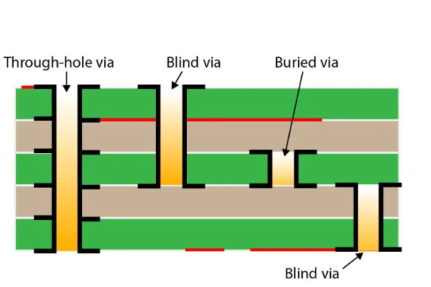
Blind vias are a type of vertical interconnect access (via) used in multilayer PCBs to connect an external layer to one or more internal layers without penetrating the full thickness of the board. Unlike through-hole vias, blind vias save space and allow for denser routing, making them ideal for compact, high-performance designs.
The materials used in PCB construction play a significant role in the performance of blind vias. They affect how well the via conducts electricity, withstands thermal stress, and maintains signal integrity at high frequencies. Poor material choices can lead to issues like delamination, poor plating adhesion, or signal loss, especially in demanding applications. By selecting high-performance PCB materials, you can ensure reliable blind vias that meet the needs of modern electronics.
Key Factors in Blind Via PCB Materials Selection
When selecting materials for PCBs with blind vias, several critical factors must be considered. These elements ensure that the vias function reliably under various conditions and during manufacturing processes like drilling and plating.
1. Dielectric Constant (Dk) and Loss Tangent (Df)
The dielectric constant (Dk) measures a material’s ability to store electrical energy, while the loss tangent (Df) indicates the energy loss as a signal passes through the material. For high-speed applications, materials with a low Dk (typically between 3.0 and 4.0) and low Df (below 0.005) are preferred. These properties minimize signal delay and loss, which is critical for blind vias in HDI designs operating at frequencies above 1 GHz.
For instance, in a 5G application, using a material with a Dk of 3.2 and a Df of 0.003 can significantly reduce signal distortion compared to a standard FR-4 material with a Dk of 4.5 and Df of 0.02. This ensures that blind vias maintain signal integrity across layers.
2. Thermal Stability and Coefficient of Thermal Expansion (CTE)
Blind vias often undergo thermal stress during manufacturing and operation. Materials with high thermal stability and a low coefficient of thermal expansion (CTE) prevent cracking or delamination around vias. A CTE mismatch between the PCB substrate and the copper plating in vias can cause mechanical failure, especially in environments with temperature fluctuations.
Materials like high-Tg (glass transition temperature) laminates, with Tg values above 170°C, offer better thermal resistance than standard FR-4 (Tg around 130°C). For applications like automotive electronics, where temperatures can exceed 125°C, a high-Tg material ensures that blind vias remain intact.
3. Mechanical Strength and Drillability
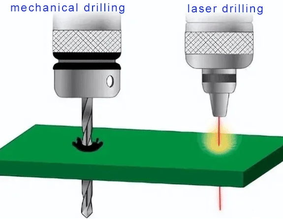
Blind vias are typically created using laser drilling or controlled-depth mechanical drilling. The material must be compatible with these processes to avoid issues like rough via walls or excessive wear on drilling tools. Softer or brittle materials can lead to poor via quality, affecting plating and conductivity.
Reinforced laminates with woven glass provide better mechanical strength and drillability compared to non-reinforced options. This is especially important for microvias (blind vias with diameters below 0.15 mm), where precision is critical.
4. Copper Plating Compatibility
After drilling, blind vias are plated with copper to establish conductivity between layers. The PCB material must support uniform copper deposition without defects like voids or poor adhesion. Materials with smooth, consistent surfaces and low moisture absorption are ideal for reliable plating.
For example, materials with a moisture absorption rate below 0.2% prevent swelling or degradation during the plating process, ensuring that blind vias maintain electrical continuity.
High-Performance PCB Materials for Blind Vias
Standard FR-4 materials may suffice for basic designs, but high-performance applications demand advanced materials tailored for blind vias. Below are some categories of high-performance PCB materials that excel in HDI designs.
1. High-Tg FR-4 Variants
High-Tg FR-4 materials are an upgraded version of standard FR-4, offering improved thermal stability with glass transition temperatures ranging from 150°C to 180°C. They are cost-effective for mid-range applications and provide decent compatibility with blind via manufacturing. These materials are suitable for consumer electronics where moderate performance is needed.
2. Polyimide-Based Materials
Polyimide laminates are known for their exceptional thermal resistance, with operating temperatures up to 260°C. They also have a low CTE, making them ideal for blind vias in aerospace and military applications where reliability under extreme conditions is non-negotiable. Their flexibility also supports designs with tight spacing.
3. PTFE-Based Materials
Polytetrafluoroethylene (PTFE) materials are widely used in high-frequency applications due to their low Dk (around 2.1 to 2.5) and low Df (below 0.002). These properties make them perfect for blind vias in RF and microwave circuits, where signal integrity is paramount. However, PTFE can be challenging to drill and plate, requiring specialized manufacturing processes.
4. Ceramic-Filled Laminates
Ceramic-filled materials offer a balance of thermal conductivity and electrical performance. With Dk values ranging from 3.0 to 10.0, they are versatile for mixed-signal designs. Their high thermal conductivity (up to 3 W/mK) helps dissipate heat around blind vias, making them suitable for power electronics.
Blind Via Material Compatibility: Matching Materials to Design Needs
Compatibility between the PCB substrate, copper plating, and manufacturing processes is essential for reliable blind vias. Here’s how to ensure that your material choices align with your design requirements.
1. Matching Material to Frequency Requirements
For high-frequency designs, prioritize materials with low dielectric loss. A mismatch can cause signal degradation in blind vias, leading to data errors. For example, in a 10 GHz application, a PTFE-based material with a Df of 0.0015 outperforms a high-Tg FR-4 with a Df of 0.015 by reducing signal attenuation by up to 30%.
2. Considering Layer Count and Via Depth
In multilayer PCBs with blind vias spanning several layers, material uniformity is critical. Variations in material properties across layers can cause uneven drilling or plating. Choose materials with consistent Dk and CTE values across the stack-up to maintain via reliability.
3. Environmental and Regulatory Compliance
For applications in regulated industries like medical or automotive, ensure that materials comply with standards such as RoHS (Restriction of Hazardous Substances). Halogen-free laminates are often preferred in these sectors to minimize environmental impact while maintaining performance.
PCB Material Selection Guide for Blind Vias
Follow this step-by-step guide to choose the right materials for reliable blind vias in your PCB designs.
Step 1: Define Application Requirements
Start by identifying the electrical, thermal, and mechanical demands of your project. For high-speed digital circuits, focus on low Dk and Df. For high-power applications, prioritize thermal conductivity and high Tg.
Step 2: Evaluate Manufacturing Constraints
Consider the capabilities of your manufacturing process. Laser drilling for microvias requires materials with low ablation thresholds, while mechanical drilling may need tougher laminates to avoid damage.
Step 3: Test Material Performance
Before full-scale production, prototype your design with the selected material. Test for signal integrity, thermal cycling (e.g., -40°C to 125°C for 100 cycles), and via reliability to confirm that blind vias perform as expected.
Step 4: Balance Cost and Performance
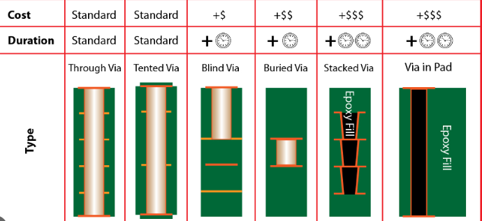
High-performance materials often come with a higher price tag. Weigh the benefits of advanced materials against budget constraints. For less demanding applications, a high-Tg FR-4 may offer sufficient reliability without breaking the bank.
Common Challenges with Blind Vias and Material Solutions
Even with careful planning, challenges can arise when designing and manufacturing blind vias. Here are some common issues and how material selection can address them.
1. Via Cracking Under Thermal Stress
Repeated heating and cooling can cause cracks in blind vias. Using materials with a low CTE (below 15 ppm/°C) minimizes stress at the via-substrate interface, reducing the risk of failure.
2. Poor Plating Adhesion
Inadequate copper plating can lead to open circuits. Materials with low moisture absorption and smooth surfaces improve adhesion during the plating process, ensuring consistent conductivity.
3. Signal Loss in High-Frequency Designs
At frequencies above 5 GHz, signal loss through blind vias becomes noticeable. Opt for materials with a Dk below 3.5 and a Df below 0.005 to keep losses under control.
Conclusion: Building Reliable Blind Vias with the Right Materials
Selecting the right materials for reliable blind vias in PCBs is a balancing act between performance, manufacturability, and cost. By understanding the key properties of high-performance PCB materials—such as dielectric constant, thermal stability, and mechanical strength—you can make informed decisions that enhance the reliability of your designs. Whether you’re working on high-frequency telecommunications or rugged automotive systems, a thoughtful approach to blind via material compatibility ensures success.
With this PCB material selection guide, you’re equipped to tackle the challenges of HDI designs and create robust, efficient circuits. Focus on matching materials to your specific needs, and don’t hesitate to test and iterate during the prototyping phase. Reliable blind vias start with the right foundation, and the right materials are the key to that foundation.