 ALLPCB


Introduction
PCB warpage represents a critical challenge in electronic design and assembly, where dimensional instability can compromise overall board reliability. This phenomenon often arises from interactions between the board structure and placed components, leading to uneven stress distribution during thermal processes. Electrical engineers must address component placement stress early in the design phase to prevent issues like solder joint failures and assembly defects. By optimizing layouts for thermal distribution design and heavy component support, designers can significantly reduce warpage risks. This guide explores the mechanisms behind warpage, practical mitigation strategies, and analytical tools like FEA analysis. Understanding these elements ensures robust performance in high-density applications.
What Is PCB Warpage and Why It Matters
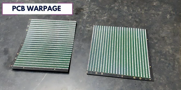
PCB warpage refers to the out-of-plane deformation of a printed circuit board, manifesting as bow or twist that deviates from flatness. This deformation typically results from residual stresses accumulated during fabrication, lamination, or assembly phases. In modern electronics, where surface-mount technology dominates, even minor warpage can misalign components during reflow soldering, causing bridging or open joints. For electrical engineers, maintaining flatness is essential for automated pick-and-place accuracy and long-term reliability under thermal cycling. Industry standards such as IPC-6012 outline acceptability criteria for warpage, emphasizing its impact on yield and performance. Neglecting warpage control can escalate costs through rework and field failures.
Warpage matters particularly in multilayer boards with fine-pitch components, where tolerances are tight. Uneven stress from component placement exacerbates this, altering contact between the board and conveyor during assembly. Engineers must consider warpage in the context of overall system integrity, as it influences signal integrity and mechanical stability. Proactive design adjustments prevent propagation of stresses that could lead to delamination or cracking over time.
Causes of PCB Warpage Linked to Component Placement
Component placement introduces mechanical and thermal loads that contribute to warpage through asymmetric stress fields. Heavy or densely packed components on one side create localized bending moments, especially if not balanced across the board. During reflow, differential expansion between the PCB substrate and components generates component placement stress, pulling the board into curvature. Uneven copper distribution beneath components further amplifies this by creating thermal gradients.
Thermal mismatch plays a central role, as coefficients of thermal expansion differ between silicon dies, solder, and laminate materials. When components are clustered near edges or corners, the board experiences higher tensile or compressive forces on those regions. Hygroscopic effects from absorbed moisture can compound these issues, swelling layers unevenly and promoting twist. Fabrication-induced stresses, like those from drilling or plating, interact with placement patterns to worsen deformation.
Technical Principles of Stress in Component Placement
The core mechanism driving warpage involves hygro-thermo-mechanical stresses governed by material properties and geometry. Component placement stress arises primarily from shear and peel forces at solder joints during temperature excursions. Finite element models reveal that off-center heavy components induce torque, rotating the board around its neutral axis. Balancing mass distribution mitigates this by equalizing moments of inertia across the plane.
Thermal distribution design influences warpage by controlling heat flow paths. Concentrated power dissipation under components creates hotspots, leading to localized expansion and buckling. Vias and ground planes act as heat spreaders, but poor routing can channel heat unevenly, stressing adjacent areas. Engineers must analyze stackup symmetry to ensure core and prepreg layers respond uniformly to temperature changes.
Practical Solutions for Minimizing Component Placement Stress
To counter component placement stress, adopt symmetric layouts where possible, mirroring components across the board's centerline. Distribute high-power devices evenly to avoid thermal hotspots that warp thin sections. Route traces and pours to balance copper weight on opposing layers, reducing differential shrinkage during cool-down. These steps align with principles in IPC-9641 for maintaining flatness under elevated temperatures.
Support structures during assembly further alleviate stress. Use pallets or fixtures to constrain board movement in reflow ovens, applying even pressure without inducing new distortions. Pre-baking boards removes moisture, preventing vapor-induced expansion that interacts with placed components. Iterative design reviews incorporating placement simulations help identify stress-prone configurations early.
Thermal Distribution Design for Warpage Reduction
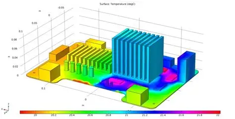
Thermal distribution design optimizes heat dissipation to minimize gradients that cause warpage. Implement embedded heat spreaders or thermal vias under hot components to equalize temperatures across the board. Layered copper planes with staggered patterns promote lateral conduction, countering vertical expansion differences. Engineers should model airflow paths in enclosures to ensure convective cooling supports board-level uniformity.
Avoid clustering heat-generating components, as this concentrates expansion in localized zones, bowing the substrate. Instead, intersperse them with lower-power parts, using fill patterns to fine-tune effective CTE. Compliance with JEDEC guidelines for reflow profiles complements these designs by ramping temperatures gradually, allowing stress relaxation. This holistic approach integrates thermal management with mechanical stability.
Heavy Component Support Techniques
Heavy component support requires strategic placement and mechanical aids to prevent sagging or tilting that induces warpage. Position large devices like connectors or capacitors near the board center, where flexural rigidity is highest. Reinforce mounting areas with additional stitching vias or edge bevels to distribute loads. During handling, employ edge supports or vacuum fixtures to maintain planarity.
For multilayer boards, thicker cores under heavy components enhance stiffness without overall weight penalties. Symmetrical bracketing on both sides prevents cantilever effects. Assembly jigs with adjustable pins provide localized backing, especially for BGAs prone to stress concentration. These techniques ensure heavy component support integrates seamlessly with warpage control.
Leveraging FEA Analysis for Predictive Design
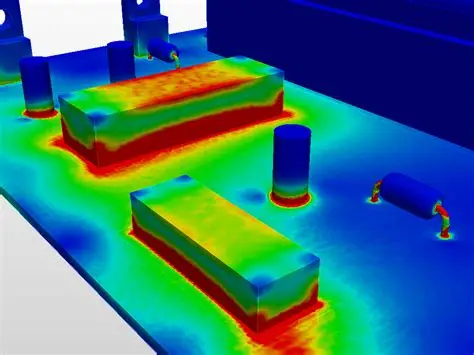
FEA analysis stands as a powerful tool for quantifying component placement stress before prototyping. By inputting material properties, geometry, and boundary conditions, simulations predict warpage under reflow cycles. Mesh refinement around component edges captures local stress peaks accurately. Engineers iterate layouts virtually, adjusting for minimal peak strains.
Couple FEA with thermal solvers to model coupled field effects, revealing how thermal distribution design influences deformation. Validate models against shadow moiré measurements for accuracy. This predictive capability reduces physical trials, aligning designs with standards like IPC-6012. FEA empowers data-driven decisions on heavy component support and overall symmetry.
Best Practices Integration
Combine these strategies into a cohesive workflow: start with stackup balancing, proceed to symmetric placement, and verify via FEA analysis. Document thermal profiles and support requirements in fabrication notes. Post-assembly inspections using laser profilometers confirm compliance. Regular design audits refine approaches for evolving component densities.
Conclusion
Minimizing PCB warpage demands attention to component placement stress through balanced layouts and thermal distribution design. Heavy component support via strategic positioning and fixtures prevents mechanical overloads, while FEA analysis provides foresight into potential failures. Adhering to standards ensures reliability across thermal cycles. Electrical engineers who integrate these practices achieve higher yields and durable assemblies. Proactive warpage management elevates design quality from good to exceptional.
FAQs
Q1: How does component placement stress contribute to PCB warpage?
A1: Component placement stress arises from uneven mechanical loads and thermal expansion mismatches during reflow. Asymmetric arrangements of components create bending moments, deforming the board. Balancing placements distributes forces evenly, reducing warpage as per industry guidelines. This prevents solder defects and enhances assembly precision.
Q2: What role does thermal distribution design play in warpage prevention?
A2: Thermal distribution design equalizes heat across the PCB, minimizing gradients that cause differential expansion. Use vias and planes to spread dissipation from components. Poor design leads to hotspots and stress concentrations. Optimized layouts maintain flatness under operational temperatures.
Q3: Why is heavy component support critical for minimizing stress?
A3: Heavy component support counters gravitational and thermal loads that warp thin boards. Central placement and reinforcements distribute weight uniformly. Fixtures during assembly provide stability. Neglect leads to localized deformation and joint failures. Proper techniques ensure structural integrity.
Q4: How can FEA analysis help with PCB warpage?
A4: FEA analysis simulates warpage from component placement and thermal loads pre-fabrication. It identifies high-stress zones for redesign. Coupled thermo-mechanical models predict reflow behavior accurately. This tool optimizes thermal distribution design and heavy component support iteratively. Validation refines predictions.
References
IPC-6012E — Qualification and Performance Specification for Rigid Printed Boards. IPC, 2017
IPC-9641 — High Temperature Printed Board Flatness Guideline. IPC, 2013
JEDEC J-STD-020E — Moisture/Reflow Sensitivity Classification. JEDEC, 2014


