ALLPCB


Are you new to PCB design and wondering how to create effective PCB traces? PCB trace design is a critical part of building reliable and efficient circuit boards. In this ultimate guide for beginners, we’ll walk you through the essentials of PCB trace design, covering trace width, routing, vias, pads, copper, impedance, and current capacity. Whether you're a hobbyist or an aspiring engineer, this detailed guide will help you understand the fundamentals and apply them to your projects.
Let’s dive into the world of PCB traces and explore how to design them for optimal performance. From understanding the basics to mastering advanced concepts, this guide has everything you need to get started.
What Are PCB Traces and Why Are They Important?
PCB traces are the thin copper pathways on a printed circuit board (PCB) that connect different components, such as resistors, capacitors, and integrated circuits. Think of them as the "wires" of your circuit board, carrying electrical signals and power between parts. Without properly designed traces, your PCB could suffer from issues like signal loss, overheating, or even complete failure.
The design of these traces directly impacts the performance of your board. Factors like trace width, spacing, and routing affect how well signals travel, how much current the trace can handle, and how much interference or noise is introduced. For beginners, mastering PCB trace design is the foundation of creating functional and reliable electronics.

Key Elements of PCB Trace Design for Beginners
Designing PCB traces involves several important factors. Let’s break them down into manageable sections so you can understand each aspect and apply it to your projects.
1. Trace Width: Balancing Current and Heat
Trace width refers to how wide the copper pathway is on your PCB. The width of a trace is crucial because it determines how much current it can carry without overheating. If a trace is too narrow for the current passing through it, it can heat up, potentially damaging the board or causing failure.
A common guideline for beginners is to use a trace width calculator based on industry standards like IPC-2221. For example, a trace carrying 1 Amp of current on a standard 1 oz copper layer (common in most PCBs) typically needs a width of about 20 mils (0.02 inches) to keep temperature rise below 10°C. For higher currents, like 3 Amps, you might need a width of 50 mils or more, depending on the copper thickness and ambient conditions.
Always consider the current capacity of your trace during design. Wider traces can handle more current, but they take up more space on the board. Finding the right balance is key.

2. Routing: Planning the Path of Your Traces
Routing is the process of planning the paths your traces will take on the PCB. Good routing ensures that signals travel efficiently without interference and that the board remains organized and easy to manufacture.
For beginners, follow these basic routing tips:
- Keep traces as short and direct as possible to minimize signal delay and resistance.
- Avoid sharp 90-degree angles in your traces. Instead, use 45-degree angles or curves to reduce signal reflection and improve manufacturability.
- Separate high-speed signal traces from power and ground traces to avoid noise interference.
Proper routing also means considering the layout of your components. Place components logically so that traces don’t have to cross unnecessarily, which can complicate the design and increase the risk of errors.
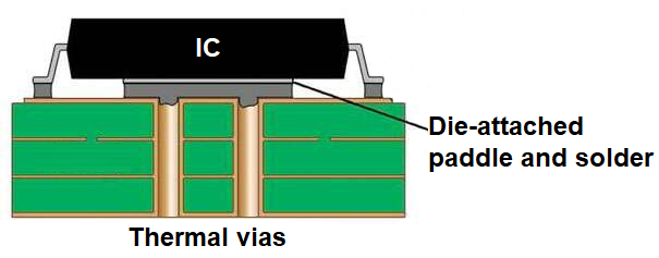
3. Vias: Connecting Layers in Multilayer PCBs
Vias are small holes in a PCB that allow traces to connect between different layers of the board. In multilayer PCBs, vias are essential for creating compact designs by routing traces vertically through the board.
There are three main types of vias:
- Through-Hole Vias: These go through all layers of the board and are the most common type.
- Blind Vias: These connect an outer layer to an inner layer but don’t go through the entire board.
- Buried Vias: These are hidden inside the board, connecting only internal layers.
For beginners, start with through-hole vias as they are easier to work with. Keep in mind that vias add resistance and can affect signal integrity, so use them sparingly in high-speed designs. Also, ensure vias are placed away from high-current areas to avoid thermal issues.

4. Pads: Connecting Components to Traces
Pads are the small copper areas on a PCB where components are soldered to connect with traces. Designing pads correctly ensures strong connections and reliable performance.
Pad size depends on the component type. For example, surface-mount components need smaller, precisely shaped pads, while through-hole components require larger pads with holes for leads. A typical pad for a 0805 surface-mount resistor might be around 1.2 mm by 1.5 mm, but always check the component datasheet for exact dimensions.
Ensure pads are not too close to each other to avoid solder bridges during assembly. A minimum spacing of 0.2 mm between pads is a good starting point for most designs.
5. Copper Thickness: Understanding Weight and Performance
Copper thickness, often referred to as copper weight, is measured in ounces per square foot (oz/ft2). Common weights are 1 oz and 2 oz, with 1 oz being standard for most beginner projects. This translates to a thickness of about 35 micrometers for 1 oz copper.
Thicker copper (like 2 oz or more) can carry higher currents and is more durable, but it’s also more expensive and harder to etch precisely. For most low-power designs, 1 oz copper is sufficient. However, for power electronics handling currents above 5 Amps, consider using 2 oz copper or wider traces to manage heat.
Keep in mind that copper thickness also affects impedance, which we’ll discuss next. Balancing cost and performance is essential when choosing copper weight.
Related Reading: 1 oz vs 2 oz Copper PCB: Which Thickness Should You Choose?
6. Impedance: Controlling Signal Integrity
Impedance is a measure of how much a trace resists the flow of alternating current (AC) signals, especially in high-speed designs. It’s influenced by trace width, copper thickness, and the dielectric material of the PCB.
For beginners working on low-speed circuits (like simple LED projects), impedance might not be a major concern. However, in high-speed designs (like USB or HDMI interfaces), maintaining consistent impedance is critical to prevent signal distortion. A common target impedance for high-speed signals is 50 ohms, often achieved by adjusting trace width to around 6-8 mils on a standard FR4 board with 1 oz copper.
Use impedance calculators or design software to determine the correct trace dimensions for your specific application. Poor impedance control can lead to signal reflections and data errors.
7. Current Capacity: Preventing Overheating
Current capacity is the maximum amount of current a trace can handle without overheating or failing. As mentioned earlier, trace width and copper thickness play a big role here. The IPC-2221 standard provides detailed tables for calculating current capacity based on trace dimensions and temperature rise.
For example, a 10-mil wide trace with 1 oz copper can safely carry about 0.5 Amps with a 10°C temperature rise. If your circuit demands more current, increase the trace width or copper weight. Overloading a trace can cause it to burn out, so always design with a safety margin—aim for a temperature rise of no more than 10-20°C under normal operating conditions.
Related Reading: The Ultimate Guide to PCB Trace Width for Beginners
Best Practices for PCB Trace Design
Now that you understand the key elements, here are some best practices to follow when designing PCB traces:
- Use Design Software: Tools with built-in trace width calculators and routing assistants can simplify the process for beginners.
- Follow Manufacturer Guidelines: Check the design rules provided by your PCB fabrication service to ensure your traces meet minimum width and spacing requirements (often 6 mils for standard processes).
- Test Your Design: Before finalizing, simulate your PCB design to check for potential issues like excessive heat or signal interference.
- Plan for Heat Dissipation: Add thermal reliefs or wider traces in high-current areas to prevent overheating.
- Keep Ground Planes in Mind: A solid ground plane under your traces can reduce noise and improve signal integrity.

Common Mistakes to Avoid in PCB Trace Design
As a beginner, it’s easy to make mistakes in PCB trace design. Here are some common pitfalls and how to avoid them:
- Underestimating Current Needs: Always calculate the expected current and design traces accordingly to avoid overheating.
- Poor Spacing: Traces too close together can cause crosstalk or short circuits. Maintain at least 6-8 mils spacing for standard designs.
- Ignoring Signal Integrity: For high-speed signals, pay attention to impedance and avoid unnecessary vias or sharp corners.
- Overcomplicating Routing: Keep your design simple and organized to make troubleshooting and manufacturing easier.
Conclusion: Start Designing Your PCB Traces with Confidence
PCB trace design might seem complex at first, but with the right knowledge and tools, it becomes an achievable task for beginners. By understanding trace width, routing, vias, pads, copper thickness, impedance, and current capacity, you can create reliable and efficient circuit boards for your projects. Remember to use industry standards, leverage design software, and always double-check your work to avoid common mistakes.
With this ultimate guide, you’re now equipped to tackle PCB trace design head-on. Start small, practice often, and watch your skills grow as you build more advanced circuits. Your journey into PCB design has just begun, and every trace you design brings you one step closer to mastering the art of electronics.