 ALLPCB


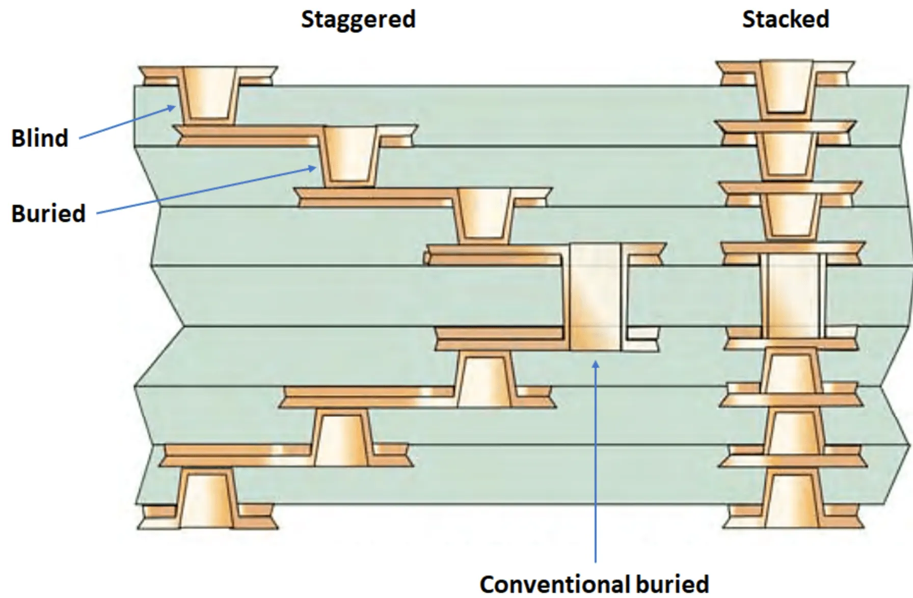
In the world of PCB design, choosing the right type of via is crucial for creating efficient, high-performance boards, especially in High-Density Interconnect (HDI) technology. So, what are the key differences between microvias and stacked vias? Microvias are small, laser-drilled holes (typically less than 0.15 mm in diameter) used to connect adjacent layers in HDI PCBs, offering space-saving and improved signal integrity. Stacked vias, on the other hand, are a configuration of microvias placed directly on top of each other to connect multiple layers, often used in complex, multilayer designs. While both are essential for modern PCB layouts, their applications, manufacturing processes, and performance impacts differ significantly.
In this comprehensive guide, we’ll dive deep into the distinctions between microvias and stacked vias, exploring their roles in PCB design, advantages, challenges, and best use cases. Whether you’re an engineer working on compact electronics or a designer optimizing for signal speed, this blog will help you make informed decisions for your next project.
What Are Microvias in PCB Design?
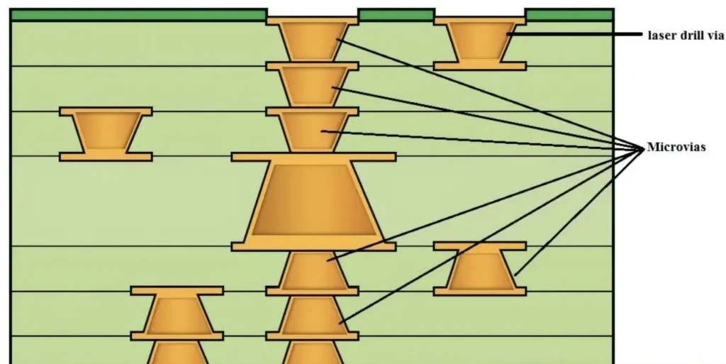
Microvias are tiny holes in a printed circuit board, usually with a diameter of less than 0.15 mm (or 6 mils), created using laser drilling technology. Unlike traditional through-hole vias that span the entire thickness of a PCB, microvias are designed to connect only adjacent layers or a few layers in HDI boards. Their small size and precision make them a cornerstone of modern PCB miniaturization, allowing designers to pack more components into smaller spaces.
Microvias are often used in applications where space is limited, such as smartphones, wearables, and medical devices. They typically have a low aspect ratio (depth-to-diameter ratio) of around 0.75:1 to 1:1, which ensures better reliability during manufacturing. This small ratio also helps reduce signal loss and parasitic capacitance, critical for high-speed circuits operating at frequencies above 1 GHz.
What Are Stacked Vias in PCB Design?
Stacked vias are a specific arrangement of microvias where multiple microvias are placed directly on top of each other to form a vertical connection across several layers of a PCB. This configuration is common in HDI technology, especially for boards with high layer counts (often 8 or more layers). By stacking microvias, designers can create a continuous path for signals or power without using larger through-hole vias, saving valuable board space.
Stacked vias are ideal for complex designs with fine-pitch components like Ball Grid Arrays (BGAs) with pitches as small as 0.4 mm. However, their vertical alignment requires precise manufacturing to avoid issues like misalignment or poor plating, which can impact reliability. Stacked vias also tend to have higher fabrication costs due to the multiple laser drilling and plating steps involved.
Key Differences Between Microvias and Stacked Vias
While both microvias and stacked vias are integral to HDI PCB design, they serve different purposes and come with unique characteristics. Below, we break down their differences across several critical factors:
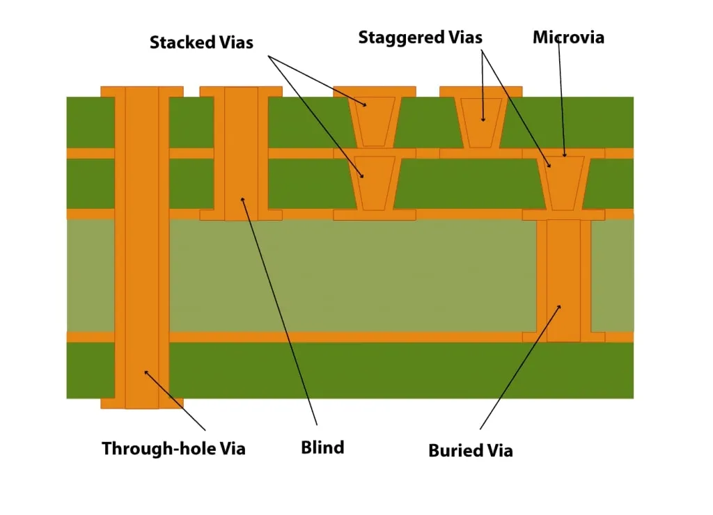
1. Structure and Placement
- Microvias: These are individual small vias that typically connect two adjacent layers or span a short depth in the PCB. They can be placed in various configurations, including staggered patterns, to optimize routing.
- Stacked Vias: These are a series of microvias aligned vertically to connect multiple layers. Their placement is more constrained due to the need for precise alignment during manufacturing.
2. Manufacturing Process
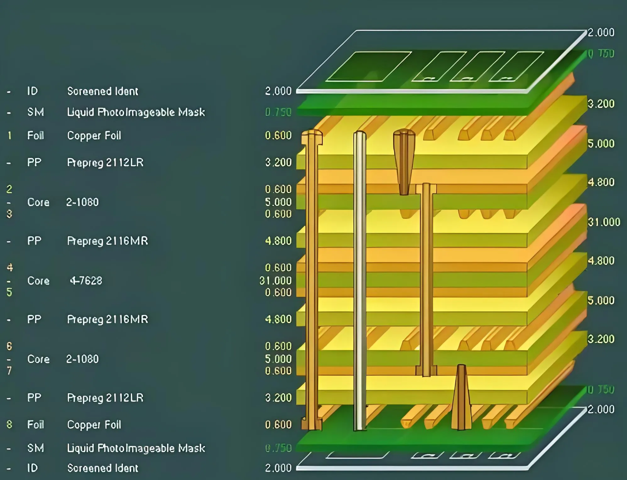
- Microvias: Created using laser drilling, microvias require fewer steps if they only connect adjacent layers. They are often filled with conductive material or copper to ensure a reliable connection.
- Stacked Vias: Manufacturing stacked vias involves multiple laser drilling and plating cycles for each layer, increasing complexity and cost. Misalignment during stacking can lead to open circuits or weak connections.
3. Space Efficiency
- Microvias: Their small size (often 0.1 mm or less) allows for high-density routing, freeing up space for additional components or traces. They are ideal for compact designs.
- Stacked Vias: While also space-efficient due to their use of microvias, stacked vias enable connections across multiple layers without occupying extra horizontal space, making them suitable for multilayer boards.
4. Signal Integrity and Performance
- Microvias: With their shorter length and smaller diameter, microvias reduce signal loss and parasitic effects like inductance and capacitance. This makes them excellent for high-speed signals, often supporting data rates up to 10 Gbps or higher.
- Stacked Vias: While effective for multilayer routing, stacked vias can introduce slightly higher signal degradation due to their longer vertical path. Careful design is needed to minimize impedance mismatches, especially at frequencies above 5 GHz.
5. Cost and Complexity
- Microvias: Generally less expensive when used individually or in simpler configurations. Costs increase with the number of layers and via density.
- Stacked Vias: More costly due to the need for precise alignment and multiple manufacturing steps. They are often reserved for high-end applications where space and performance are critical.
Advantages and Challenges of Microvias in HDI PCB Design
Advantages of Microvias
- Compact Size: With diameters as small as 0.1 mm, microvias allow for tighter component placement and finer trace widths, often down to 0.075 mm (3 mils).
- Improved Signal Integrity: Their short length minimizes signal delay and loss, crucial for high-frequency designs operating at 2.4 GHz or higher.
- Flexibility: Microvias can be used in various configurations, such as staggered or single-layer connections, to suit different design needs.
Challenges of Microvias
- Manufacturing Limits: Laser drilling microvias with aspect ratios beyond 1:1 can lead to reliability issues like incomplete plating or voids.
- Thermal Stress: Microvias are more susceptible to cracking under thermal cycling, especially in boards exposed to temperatures above 125°C during operation or reflow soldering.
Advantages and Challenges of Stacked Vias in HDI PCB Design
Advantages of Stacked Vias
- Multilayer Connectivity: Stacked vias enable direct connections across multiple layers (up to 6 or more in advanced HDI designs), reducing the need for larger vias or additional routing space.
- Space Optimization: They are essential for routing fine-pitch components like BGAs with 0.5 mm or smaller pitches, common in modern electronics.
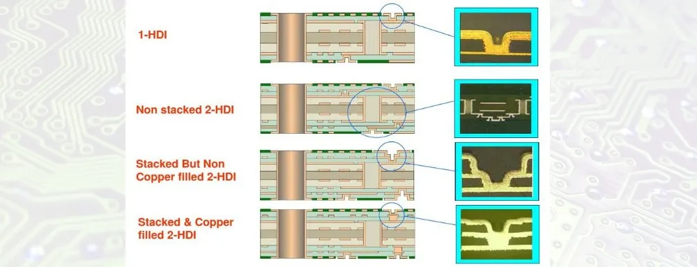
- Supports Complex Designs: Stacked vias are a key enabler of technologies like Every Layer Interconnection (ELIC), where connections span all layers of a PCB.
Challenges of Stacked Vias
- Higher Cost: The multiple drilling and plating steps required for stacked vias can increase production costs by 20-30% compared to simpler via structures.
- Reliability Concerns: Misalignment or poor copper filling in stacked vias can lead to electrical failures, especially under mechanical or thermal stress.
- Design Constraints: Stacked vias require careful planning to avoid signal integrity issues, such as impedance discontinuities at layer transitions.
When to Use Microvias vs. Stacked Vias in PCB Design
Choosing between microvias and stacked vias depends on the specific requirements of your PCB project. Here are some guidelines to help you decide:
- Use Microvias When: Your design focuses on connecting adjacent layers in a compact board with limited layer count (e.g., 4-6 layers). They are ideal for high-speed applications where signal integrity is a priority, such as in RF circuits or mobile devices.
- Use Stacked Vias When: You’re working on a multilayer HDI board (8+ layers) that requires vertical connections across several layers. Stacked vias are best for complex designs with fine-pitch components or when implementing advanced HDI techniques like ELIC.
For example, in a smartphone PCB, microvias might be used to connect the top layer to the first inner layer for routing high-speed data lines at 5 Gbps. In contrast, stacked vias could be employed to connect power or ground planes across 10 layers, ensuring efficient power distribution without sacrificing board space.
Best Practices for Designing with Microvias and Stacked Vias
To maximize the benefits of microvias and stacked vias while minimizing potential issues, consider the following design tips:
- Maintain Aspect Ratios: Keep the aspect ratio of microvias below 1:1 (ideally 0.75:1) to ensure reliable plating and filling during manufacturing.
- Plan for Thermal Management: Use thermal vias or heat dissipation strategies to protect microvias and stacked vias from stress during soldering or operation at high temperatures (above 100°C).
- Optimize Stackup Design: Work closely with your fabrication partner to define a stackup that supports the use of stacked vias, ensuring proper alignment and layer transitions for signal integrity.
- Simulate Signal Performance: Use simulation tools to analyze impedance and signal loss, especially for stacked vias in high-frequency designs operating above 1 GHz.
Conclusion: Making the Right Choice for Your HDI PCB Design
Understanding the differences between microvias and stacked vias is essential for creating efficient, reliable, and high-performance HDI PCBs. Microvias offer a compact, cost-effective solution for connecting adjacent layers with excellent signal integrity, making them perfect for simpler, high-speed designs. Stacked vias, while more complex and costly, provide the multilayer connectivity needed for advanced, space-constrained applications with fine-pitch components.
By carefully considering factors like layer count, signal requirements, and manufacturing capabilities, you can select the right via type for your project. Whether you’re designing a compact wearable device or a complex server board, leveraging the strengths of microvias and stacked vias will help you achieve optimal results in your PCB layout.
At ALLPCB, we’re committed to supporting your HDI PCB projects with advanced manufacturing solutions tailored to your needs. From microvia drilling to stacked via configurations, our expertise ensures your designs are brought to life with precision and reliability.


