In the fast-evolving world of electronics, achieving optimal PCB performance is crucial for engineers and designers. One powerful technology that can significantly enhance your printed circuit board (PCB) designs is direct imaging, often referred to as Laser Direct Imaging (LDI). But how does PCB direct imaging improve signal integrity, and why is it a game-changer for high-frequency PCB design? In this blog, we’ll dive deep into the signal integrity benefits of LDI, explore its impact on PCB trace accuracy and impedance control, and provide actionable insights to help you maximize your PCB performance.
Whether you’re working on high-speed digital circuits or complex RF applications, understanding the advantages of LDI signal performance can elevate your designs. Let’s explore this cutting-edge technology and uncover how it ensures precision, reliability, and efficiency in modern PCB manufacturing.
What is PCB Direct Imaging and Why Does It Matter?
PCB direct imaging, or LDI, is a modern manufacturing technique that uses laser technology to directly transfer circuit patterns onto a PCB substrate. Unlike traditional photolithography, which relies on physical masks and can introduce alignment errors, LDI offers unparalleled precision by eliminating the need for intermediate steps. This results in finer traces, tighter tolerances, and better overall accuracy in the PCB layout.
Why does this matter for signal integrity? In high-frequency PCB design, even the smallest deviation in trace width or spacing can lead to signal distortion, crosstalk, or impedance mismatches. With LDI, engineers can achieve consistent and accurate trace geometries, ensuring that signals travel through the board with minimal interference. This is especially critical for applications like 5G, automotive radar, and IoT devices, where high-speed data transmission is non-negotiable.
Signal Integrity Benefits of PCB Direct Imaging
Signal integrity refers to the quality and reliability of electrical signals as they travel through a PCB. Poor signal integrity can result in data errors, signal loss, or system failures. PCB direct imaging plays a vital role in maintaining signal integrity by addressing several key factors. Let’s break down the benefits:
1. Enhanced PCB Trace Accuracy
One of the standout advantages of LDI is its ability to produce highly accurate trace patterns. Traditional imaging methods often result in trace width variations of up to 10-15%, which can disrupt signal timing in high-frequency designs. In contrast, LDI achieves tolerances as tight as ±2%, ensuring that traces are uniform and precise.
For instance, in a high-speed design operating at 10 GHz, a trace width variation of just 0.1 mil can alter the characteristic impedance by several ohms, leading to signal reflections. With LDI, such deviations are minimized, providing consistent signal paths and reducing the risk of performance issues. This level of PCB trace accuracy is essential for maintaining signal integrity in demanding applications.
2. Superior Impedance Control for PCB Designs
Impedance control is a critical aspect of high-frequency PCB design. Mismatched impedance can cause signal reflections, leading to data corruption or loss. LDI ensures precise control over trace dimensions and spacing, which directly impacts the characteristic impedance of transmission lines.
For example, a typical microstrip line in a high-frequency PCB might require a characteristic impedance of 50 ohms. Achieving this requires exact trace widths and dielectric thicknesses. LDI’s precision allows manufacturers to maintain these parameters within tight tolerances, ensuring that impedance remains consistent across the board. This results in cleaner signal transmission and reduced noise, a key factor for LDI signal performance.
3. Reduced Crosstalk in High-Frequency PCB Design
Crosstalk occurs when signals from adjacent traces interfere with each other, a common issue in densely packed high-frequency designs. The precision of PCB direct imaging allows for tighter spacing between traces without sacrificing signal quality. By maintaining uniform trace geometries and minimizing deviations, LDI reduces the likelihood of electromagnetic interference (EMI) between neighboring lines.
In practical terms, this means you can design more compact boards for applications like mobile devices or wearables without worrying about signal degradation. For high-frequency PCB design, where frequencies often exceed 1 GHz, this benefit is invaluable for maintaining system reliability.
4. Improved Layer-to-Layer Registration
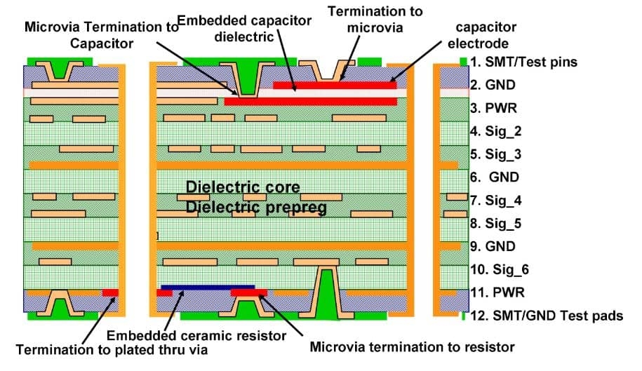
In multilayer PCBs, alignment between layers is critical for signal integrity. Misalignment can lead to via mismatches or inconsistent signal paths, especially in high-speed designs. LDI technology ensures precise layer-to-layer registration by directly imaging each layer with laser accuracy, reducing registration errors to less than 1 mil.
This precision is particularly important for impedance control in multilayer boards, where signal paths often transition between layers. With LDI, you can trust that your design’s integrity is preserved, even in complex configurations.
How LDI Signal Performance Supports High-Frequency PCB Design
High-frequency PCB design comes with unique challenges, including signal loss, phase distortion, and EMI. Operating at frequencies above 100 MHz demands meticulous attention to detail, and this is where LDI signal performance shines. Here’s how it supports high-frequency applications:
1. Minimized Signal Loss
At high frequencies, signal loss due to skin effect and dielectric absorption becomes a significant concern. The skin effect causes current to flow near the surface of conductors, increasing resistance if traces are uneven or poorly defined. LDI’s ability to create smooth, precise traces reduces surface roughness, minimizing signal loss and ensuring efficient transmission.
For example, in a 5G application operating at 28 GHz, signal loss can exceed 1 dB per inch if trace quality is subpar. With LDI, manufacturers can achieve smoother copper surfaces, cutting losses by up to 20% compared to traditional methods.
2. Support for Finer Geometries
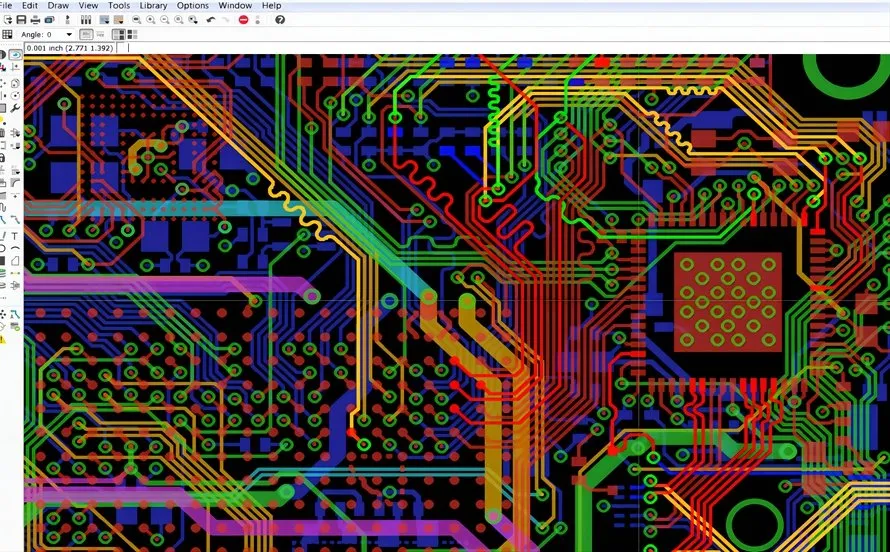
High-frequency designs often require finer trace widths and spacing to accommodate compact layouts and higher signal densities. LDI can produce traces as narrow as 1 mil (0.001 inches) with exceptional accuracy, allowing designers to push the boundaries of miniaturization without compromising signal integrity.
This capability is crucial for modern applications like RF modules, where space is limited, and performance is paramount. By leveraging PCB direct imaging, engineers can achieve the tight geometries needed for cutting-edge designs.
3. Consistency Across Production Runs
Signal integrity isn’t just about a single board; it’s about ensuring consistent performance across thousands of units. Traditional imaging methods can introduce variability between production batches due to mask wear or alignment issues. LDI eliminates these variables by using digital data to directly image each board, ensuring that every PCB meets the same high standards for trace accuracy and impedance control.
This consistency is a major advantage for high-volume production of high-frequency PCBs, where even minor deviations can lead to costly failures or recalls.
Practical Tips for Leveraging PCB Direct Imaging in Your Designs
Now that we’ve covered the signal integrity benefits of PCB direct imaging, let’s look at some practical ways to incorporate this technology into your workflow. These tips will help you maximize performance while addressing common design challenges:
- Optimize Your Design Files: Since LDI uses digital data, ensure your design files are accurate and free of errors. Use high-resolution formats to preserve the details of your layout, especially for fine traces and tight spacings.
- Collaborate with Manufacturers Early: Work closely with your PCB manufacturer to understand their LDI capabilities. Discuss specific requirements for impedance control and trace accuracy to ensure the process aligns with your design goals.
- Prioritize Material Selection: High-frequency PCB design often requires specialized materials with low dielectric constants (e.g., Dk values below 3.5). Pairing these materials with LDI ensures optimal signal performance and minimal loss.
- Simulate Signal Integrity: Use simulation tools to model signal behavior before fabrication. This allows you to identify potential issues with impedance or crosstalk and adjust your design to take full advantage of LDI precision.
Challenges and Considerations with PCB Direct Imaging
While the benefits of PCB direct imaging for signal integrity are clear, it’s important to be aware of potential challenges. Understanding these can help you make informed decisions for your projects:
- Higher Initial Costs: LDI equipment and processes can be more expensive than traditional methods, especially for small-scale production. However, the long-term benefits of improved performance and reduced rework often outweigh the upfront investment.
- Learning Curve: Transitioning to LDI may require adjustments in design workflows or software compatibility. Ensure your team is trained to handle digital imaging data and optimize designs for this technology.
- Material Compatibility: Not all PCB substrates are equally suited for LDI. Consult with your manufacturer to select materials that work well with laser imaging while meeting the needs of high-frequency applications.
Conclusion: Elevate Your PCB Performance with Direct Imaging
In the realm of modern electronics, signal integrity is the foundation of reliable, high-performing designs. PCB direct imaging, with its unmatched precision and consistency, offers significant benefits for maintaining signal quality, especially in high-frequency PCB design. From enhanced PCB trace accuracy to superior impedance control, LDI signal performance empowers engineers to tackle the challenges of high-speed and compact layouts with confidence.
By adopting this advanced technology, you can minimize signal loss, reduce crosstalk, and achieve consistent results across production runs. Whether you’re designing for 5G, automotive systems, or consumer electronics, leveraging the signal integrity benefits of PCB direct imaging can set your projects apart in terms of performance and reliability.
Ready to take your PCB designs to the next level? Explore the possibilities of LDI and see how it can transform your approach to signal integrity and high-frequency design. With the right tools and strategies, you’ll be well-equipped to meet the demands of today’s cutting-edge applications.
 ALLPCB


