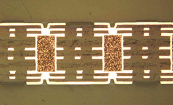
In the world of electronics, signal integrity is a cornerstone of reliable performance, especially when it comes to printed circuit boards (PCBs). Poor signal integrity can lead to data errors, system failures, and a shortened PCB lifespan. So, how do you ensure signal integrity in PCB design to minimize degradation and achieve long-term performance? The answer lies in careful design practices like controlled impedance, optimized trace routing, and effective EMI reduction strategies. In this comprehensive guide, we’ll dive deep into the essentials of signal integrity PCB design, explore techniques for minimizing signal loss in PCBs, and provide actionable tips to extend the life of your boards.
What Is Signal Integrity and Why Does It Matter for PCB Lifespan?
Signal integrity refers to the quality of an electrical signal as it travels through a PCB. When signals degrade due to factors like noise, crosstalk, or impedance mismatches, the performance of the entire system suffers. Over time, consistent signal degradation can stress components, increase heat generation, and accelerate wear, ultimately shortening the PCB’s lifespan.
Maintaining signal integrity isn’t just about immediate performance—it’s about ensuring your board operates reliably for years. Whether you’re designing for high-speed digital circuits or sensitive analog systems, focusing on signal integrity PCB design from the start can prevent costly failures down the line. Let’s explore the key factors that impact signal integrity and how they tie directly to PCB longevity.
Key Factors Affecting Signal Integrity and PCB Degradation
Several design and environmental factors can compromise signal integrity, leading to long-term degradation of a PCB. Understanding these challenges is the first step to addressing them.
1. Impedance Mismatches in PCB Design
Impedance mismatches occur when the characteristic impedance of a trace doesn’t align with the connected components or transmission lines. This mismatch causes signal reflections, which degrade signal quality and increase power loss. For high-speed designs, such as those operating at frequencies above 100 MHz, even a small mismatch (e.g., a deviation of 10% from the target 50 ohms) can lead to significant issues.
A controlled impedance PCB is essential to prevent these reflections. By carefully calculating trace width, spacing, and dielectric materials during the design phase, you can maintain consistent impedance across the board. Over time, impedance mismatches can also cause excessive heat in components, accelerating wear and reducing PCB lifespan.
2. Crosstalk Between Traces
Crosstalk happens when signals from one trace interfere with another due to electromagnetic coupling. This is especially common in densely packed boards where traces run parallel for long distances. Crosstalk introduces noise, which distorts signals and can lead to data errors. If left unchecked, the added noise can strain components like ICs, contributing to early failure.
Proper trace routing for signal integrity minimizes crosstalk by increasing spacing between high-speed traces or using ground planes as shields. This not only improves immediate performance but also reduces long-term stress on the board.
3. Signal Loss Due to Poor Trace Design
Signal loss occurs when a signal weakens as it travels along a trace, often due to resistance, dielectric losses, or long trace lengths. For instance, at frequencies above 1 GHz, dielectric losses in standard FR-4 material can reduce signal amplitude by up to 20%. This loss forces components to work harder to compensate, generating heat and wearing out faster.
Techniques for minimizing signal loss in PCBs include using low-loss materials for high-frequency designs and keeping trace lengths as short as possible. These practices help maintain signal strength and protect the board from premature aging.
4. Electromagnetic Interference (EMI)
Electromagnetic interference, or EMI, can disrupt signals and degrade performance by introducing unwanted noise. Sources of EMI include nearby electronic devices, power lines, or even poorly designed traces acting as antennas. Chronic exposure to EMI can degrade components over time, especially in sensitive analog circuits.
Implementing EMI reduction in PCB design through proper grounding, shielding, and layout techniques can significantly extend the board’s operational life by reducing noise-related stress.
Best Practices for Signal Integrity in PCB Design
Now that we’ve covered the challenges, let’s look at practical strategies to ensure signal integrity and extend PCB lifespan. These tips are tailored for engineers looking to optimize their designs for reliability and performance.
1. Design with Controlled Impedance in Mind
A controlled impedance PCB is critical for high-speed designs. Start by defining the target impedance (commonly 50 ohms for single-ended signals or 100 ohms for differential pairs) based on your components and system requirements. Use PCB design software to calculate trace width and spacing, factoring in the dielectric constant of your board material (e.g., FR-4 has a dielectric constant of about 4.5).
Additionally, maintain consistent trace geometry throughout the signal path. Avoid abrupt changes in trace width or vias that can introduce impedance discontinuities. By prioritizing controlled impedance, you reduce signal reflections and protect components from unnecessary stress.
2. Optimize Trace Routing for Signal Integrity
Effective trace routing for signal integrity is about minimizing interference and signal loss. Follow these guidelines:
- Keep high-speed traces as short and direct as possible to reduce resistance and dielectric losses.
- Avoid running high-speed traces parallel for long distances to prevent crosstalk. If unavoidable, maintain a spacing of at least 3 times the trace width.
- Use 45-degree angles instead of sharp 90-degree turns to minimize signal reflections.
- Route critical signals on inner layers near ground planes to shield them from external noise.
By carefully planning trace paths, you can enhance signal quality and reduce wear on the board over time.
3. Minimize Signal Loss with Material and Layout Choices
For minimizing signal loss in PCBs, material selection and layout play a big role. At high frequencies, standard materials like FR-4 may introduce significant dielectric losses. Consider using low-loss materials like Rogers or Isola for applications above 1 GHz, as they can cut signal loss by up to 30% compared to FR-4.
In terms of layout, avoid long trace runs and unnecessary vias, as each via can introduce a small amount of loss and reflection. When vias are needed, use back-drilling to remove unused stubs that can degrade signals. These steps help maintain signal strength and reduce thermal stress on components.
4. Implement EMI Reduction Techniques
EMI reduction in PCB design is essential for both signal integrity and long-term reliability. Here are some proven methods:
- Use solid ground planes beneath signal layers to provide a low-impedance return path and shield against external noise.
- Place decoupling capacitors close to power pins of ICs to filter out high-frequency noise. A common value for these capacitors is 0.1 μF for frequencies up to 100 MHz.
- Enclose sensitive circuits in metal shielding cans if external EMI is a concern.
- Avoid creating loops in traces or ground planes, as they can act as antennas and pick up or emit EMI.
By reducing EMI, you not only improve signal quality but also protect the PCB from long-term degradation caused by noise-induced stress.
How Signal Integrity Impacts PCB Lifespan
The connection between signal integrity and PCB lifespan is direct and significant. When signals degrade, components must compensate by drawing more power or operating under suboptimal conditions. This leads to increased heat generation, which is a primary cause of component failure. For example, a 10°C rise in operating temperature can halve the lifespan of some electronic components.
Additionally, poor signal integrity can cause intermittent errors that stress firmware or software, leading to system crashes or data corruption. Over time, these issues compound, accelerating wear on the PCB. By focusing on signal integrity PCB design, using controlled impedance PCB techniques, and optimizing trace routing for signal integrity, you create a board that operates efficiently and lasts longer.
Advanced Tips for Long-Term PCB Performance
Beyond the basics, here are some advanced strategies to further enhance signal integrity and PCB durability:
- Simulation Tools: Use signal integrity simulation software to model your design before fabrication. These tools can predict impedance mismatches, crosstalk, and signal loss, allowing you to address issues early.
- Thermal Management: Incorporate heat sinks or thermal vias to dissipate heat from high-power components, as excess heat directly impacts both signal integrity and component lifespan.
- Regular Testing: After fabrication, test your PCB for signal integrity using tools like time-domain reflectometry (TDR) to measure impedance and identify discontinuities.
These proactive measures ensure that your PCB performs reliably over an extended period, even in demanding applications.
Conclusion: Building PCBs for the Long Haul
Signal integrity is more than a design consideration—it’s a critical factor in determining the lifespan and reliability of your PCB. By prioritizing signal integrity PCB design, implementing controlled impedance PCB techniques, optimizing trace routing for signal integrity, focusing on minimizing signal loss in PCBs, and employing EMI reduction in PCB strategies, you can create boards that perform consistently over the long term.
Every design decision, from material selection to trace layout, impacts both immediate functionality and future durability. With the right approach, you can minimize degradation, reduce stress on components, and ensure your PCBs stand the test of time. Start applying these principles in your next project to achieve superior performance and reliability.
 ALLPCB


