ALLPCB


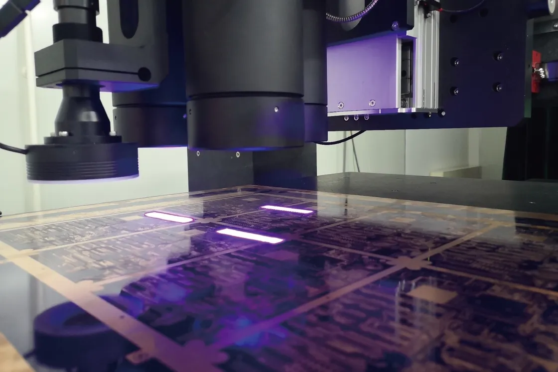
Are you looking to understand the PCB etching process and how it impacts the quality and precision of printed circuit boards? In simple terms, PCB etching is a critical step in PCB manufacturing where unwanted copper is removed from the board to create the desired circuit pattern. There are various techniques like chemical etching PCB, wet etching, and dry etching, each with unique benefits, challenges, and effects on etching tolerances. In this comprehensive guide, we’ll break down these methods, explore their impact on manufacturing, and provide actionable insights to help you choose the right approach for your project.
What Is the PCB Etching Process?
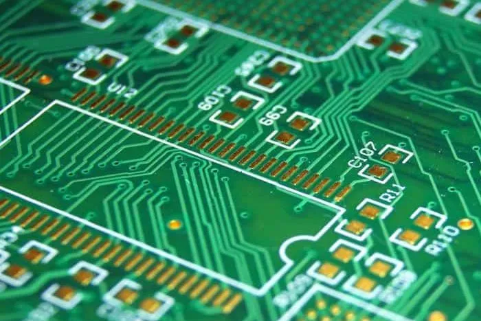
The PCB etching process is a fundamental part of creating printed circuit boards. It involves removing excess copper from a copper-clad board to form the conductive traces and pads that make up the circuit design. This process is essential for transforming a blank board into a functional component used in electronics, from smartphones to industrial machinery.
Etching can be performed using different techniques, each suited to specific applications based on factors like precision, cost, and production volume. The most common methods include chemical etching PCB (often referred to as wet etching), dry etching, and emerging technologies like laser etching. Understanding these techniques helps engineers and manufacturers achieve the desired etching tolerances and ensure high-quality results in PCB manufacturing.
Why Is PCB Etching Important?
Etching directly affects the performance and reliability of a printed circuit board. If done incorrectly, it can lead to issues like over-etching, where too much copper is removed, causing weak traces or open circuits. Under-etching, on the other hand, leaves excess copper, which can result in short circuits. Achieving precise etching tolerances—often within a range of ±10% of the trace width (e.g., ±0.001 inches for a 0.010-inch trace)—is crucial for maintaining signal integrity, especially in high-frequency applications where impedance control is critical (typically targeting 50 ohms for RF designs).
Beyond functionality, the choice of etching technique impacts production costs, turnaround times, and environmental considerations. Let’s dive into the different methods to see how they work and where they fit best in PCB manufacturing.
Types of PCB Etching Techniques
1. Chemical Etching PCB (Wet Etching)
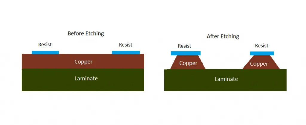
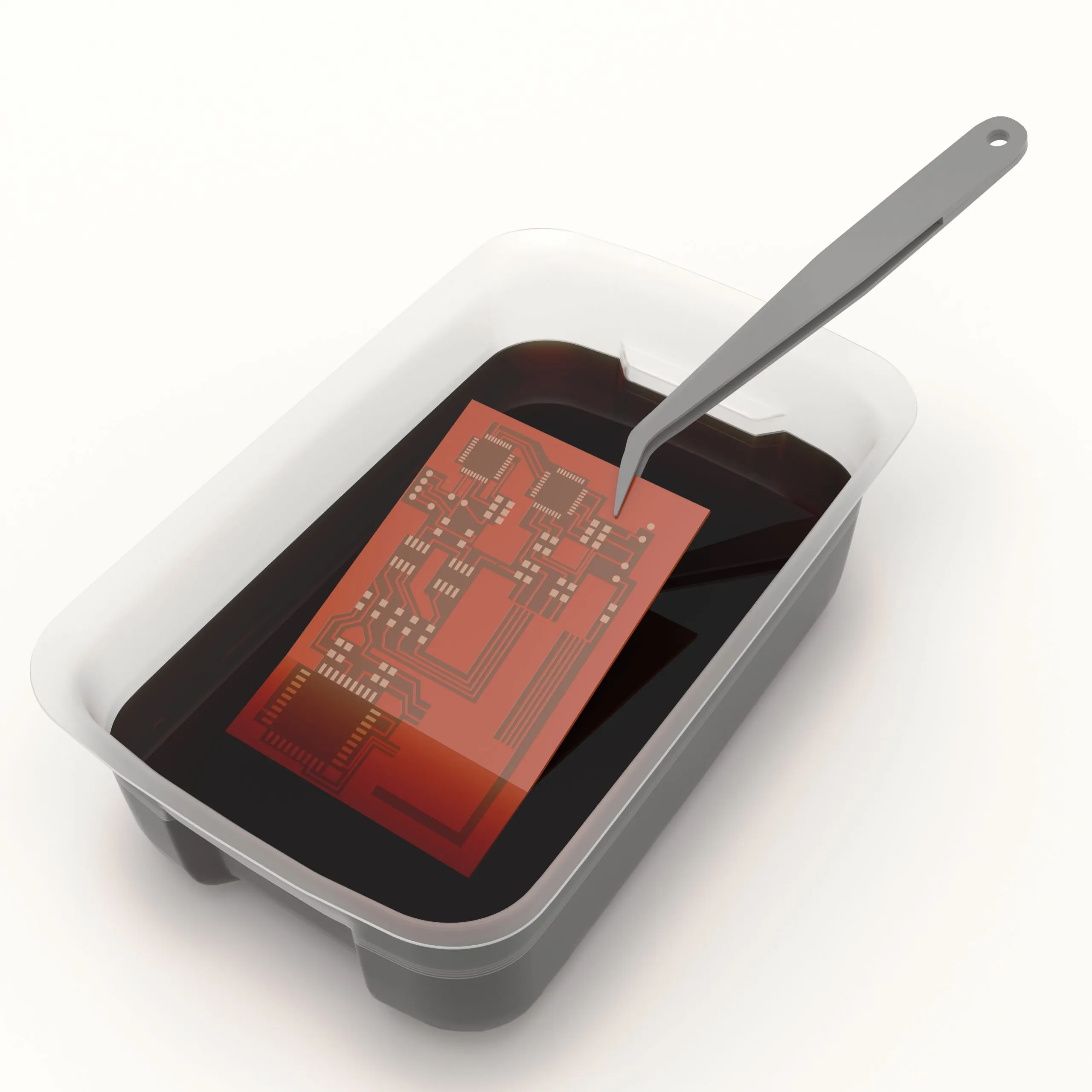
Wet etching, also known as chemical etching PCB, is the most traditional and widely used method in PCB manufacturing. In this process, the board is immersed in a chemical solution that dissolves the unprotected copper, leaving behind the circuit pattern protected by a resist layer (often a photoresist or etch-resistant ink).
How It Works:
- A resist layer is applied to the copper-clad board, covering the areas that will form the circuit traces.
- The board is submerged in an etchant solution, such as ferric chloride or ammonium persulfate, which chemically reacts with the exposed copper to remove it.
- After etching, the resist is stripped away, revealing the final copper pattern.
Advantages:
- Cost-effective for small to medium production runs.
- Simple setup, making it accessible for prototyping and hobbyists.
- Works well for standard designs with trace widths above 0.006 inches.
Challenges:
- Isotropic etching nature (etches equally in all directions) can lead to undercutting, where the etchant removes copper beneath the resist, affecting etching tolerances (typically ±0.002 inches variation).
- Slower process for high-density designs due to longer chemical reaction times.
- Environmental concerns due to the use and disposal of hazardous chemicals.
2. Dry Etching
Dry etching is a more advanced technique often used in high-precision PCB manufacturing, especially for complex, high-density interconnect (HDI) boards. Unlike wet etching, dry etching uses plasma or gaseous etchants to remove copper or other materials without liquid chemicals.
How It Works:
- The PCB is placed in a vacuum chamber where plasma (ionized gas) is generated.
- The plasma reacts with the exposed material, either through physical bombardment or chemical reaction, to remove unwanted copper.
- A mask or resist layer protects the areas that should remain intact.
Advantages:
- Highly anisotropic etching (directional), allowing for tighter etching tolerances (as low as ±0.0005 inches), ideal for fine traces below 0.003 inches.
- Better control over the process, reducing undercutting and improving precision for high-frequency designs requiring strict impedance control (e.g., 50 ohms ±5%).
- Environmentally friendlier since it avoids liquid chemical waste.
Challenges:
- Expensive equipment and setup costs, making it less viable for low-volume production.
- Requires specialized expertise and controlled environments.
- Slower for large-scale copper removal compared to wet etching.
3. Laser Etching
Laser etching is an emerging method in the PCB etching process, using focused laser beams to remove copper or other materials with extreme precision. While not as common as wet or dry etching, it’s gaining traction for specialized applications.
How It Works:
- A laser beam vaporizes the unwanted copper layer by layer, following the circuit design programmed into the system.
- No resist layer is needed in some cases, as the laser directly targets specific areas.
Advantages:
- Exceptional precision with etching tolerances as tight as ±0.0001 inches, perfect for microelectronics and ultra-fine traces (below 0.001 inches).
- No chemical waste, making it an eco-friendly option.
- Highly flexible for custom designs and rapid prototyping.
Challenges:
- Very high equipment and operational costs, limiting its use to niche applications.
- Slower for large-scale production due to the time-intensive nature of laser scanning.
- Not suitable for thick copper layers (above 2 oz or 70 microns) due to heat dissipation issues.
Etching Tolerances: Why Precision Matters in PCB Manufacturing
In PCB manufacturing, etching tolerances refer to the acceptable deviation in trace width, spacing, and other dimensions after the etching process. These tolerances are critical because even small variations can impact the board’s electrical performance, especially in high-speed or high-frequency applications.
For example, a trace width designed to be 0.008 inches with a tolerance of ±0.001 inches ensures the impedance remains within the target range (e.g., 50 ohms for differential pairs in USB or HDMI designs). If the etching process exceeds this tolerance due to undercutting or uneven etching, signal integrity issues like crosstalk or signal delay can occur, with delays potentially increasing by 10-20 picoseconds per inch of trace length.
Different etching methods offer varying levels of control over tolerances:
- Wet Etching: Tolerances typically range from ±0.001 to ±0.002 inches, suitable for standard designs but less reliable for fine-pitch components.
- Dry Etching: Achieves tighter tolerances of ±0.0005 inches, ideal for HDI boards and RF applications.
- Laser Etching: Offers the best tolerances at ±0.0001 inches, perfect for cutting-edge microelectronics.
Choosing the right etching technique depends on the design requirements, such as trace density, board complexity, and performance expectations. For instance, a simple power supply board may work fine with wet etching, while a 5G communication board demands the precision of dry or laser etching.
Factors Affecting the PCB Etching Process
Several factors influence the outcome of the PCB etching process, regardless of the technique used. Understanding these can help optimize results and minimize defects.
1. Etchant Type and Concentration
In wet etching, the type and concentration of the chemical solution significantly affect the etch rate and uniformity. For instance, ferric chloride etches at a rate of approximately 0.001 inches per minute at 40°C, while higher concentrations or temperatures can double this rate but risk over-etching.
2. Temperature and Agitation
Higher temperatures and agitation (stirring the etchant) speed up the etching process in wet methods but must be controlled to avoid uneven results. A temperature range of 35-50°C is often optimal for most chemical etchants.
3. Resist Quality
The quality and thickness of the resist layer determine how well the desired copper areas are protected. A poorly applied resist can lead to defects like pinholes, causing unintended copper removal.
4. Board Material and Copper Thickness
Standard FR-4 boards with 1 oz copper (35 microns) etch faster than thicker 2 oz copper (70 microns) layers. Thicker copper requires longer exposure to etchants or more aggressive methods, impacting production time.
Environmental and Safety Considerations in PCB Etching
The PCB etching process, particularly chemical etching PCB, raises environmental and safety concerns due to the use of hazardous materials. Wet etching chemicals like ferric chloride are toxic and require proper handling and disposal to prevent contamination. Modern PCB manufacturing facilities often implement recycling systems or use less harmful etchants like sodium persulfate to reduce environmental impact.
In contrast, dry etching and laser etching produce minimal chemical waste, making them more sustainable options. However, the high energy consumption of dry etching equipment and laser systems can offset some of these benefits. Balancing performance, cost, and environmental responsibility is a growing focus in the industry.
Choosing the Right Etching Technique for Your Project
Selecting the best etching method for your PCB project depends on several factors:
- Design Complexity: Simple designs with wider traces (above 0.006 inches) can use cost-effective wet etching. High-density designs with fine traces (below 0.003 inches) benefit from dry etching or laser methods.
- Production Volume: Wet etching suits small to medium runs due to lower setup costs. For large-scale production of complex boards, investing in dry etching may be more economical long-term.
- Budget: Wet etching is the most affordable, while dry and laser etching require significant investment in equipment and expertise.
- Performance Needs: Applications requiring precise etching tolerances and impedance control, such as high-speed digital or RF circuits, demand advanced techniques like dry etching.
By aligning the etching method with your project’s specific needs, you can optimize both quality and cost-efficiency in PCB manufacturing.
Conclusion: Mastering the PCB Etching Process for Better Results
The PCB etching process is a cornerstone of PCB manufacturing, shaping the functionality and reliability of every printed circuit board. Whether you choose chemical etching PCB through wet etching for its affordability, dry etching for its precision, or laser etching for cutting-edge applications, understanding the strengths and limitations of each technique is key to achieving the desired etching tolerances and performance.
By considering factors like design requirements, production scale, and environmental impact, you can make informed decisions that enhance the quality of your PCBs. At ALLPCB, we’re committed to supporting your projects with expert guidance and state-of-the-art manufacturing solutions tailored to your needs. Dive into the world of PCB etching with confidence, knowing you have the knowledge to create high-performing, reliable boards for any application.