ALLPCB


Introduction
Laser drilling microvias has transformed PCB fabrication by enabling the creation of high-density interconnects essential for modern electronics. This technique uses focused laser beams to form precise, small-diameter vias that connect adjacent layers without the limitations of mechanical drilling. Electrical engineers designing compact devices, such as smartphones and medical equipment, rely on the microvia drilling process to achieve tighter routing and improved signal integrity. The precision of laser ablation microvia formation minimizes heat-affected zones and ensures clean hole walls, boosting overall board reliability. Factory experience shows that integrating laser drilling into high-density interconnect (HDI) workflows significantly reduces layer count while maintaining performance. As demands for miniaturization grow, understanding laser drilling microvias becomes critical for optimizing fabrication yields.
What Are Laser Drilled Microvias and Why Do They Matter?
Laser drilled microvias are blind or buried vias with diameters typically under 150 microns, formed by ablating dielectric and copper materials with laser energy. Unlike standard through-holes, these vias connect only specific layers, allowing stacked configurations in HDI PCBs for greater interconnect density. The microvia drilling process supports aspect ratios up to 1:1, enabling vertical transitions in thin laminates without excessive plating challenges. This capability matters because it shortens signal paths, reduces parasitic inductance, and supports fine-pitch components like BGAs with 0.3 mm pitch. In fabrication, microvias facilitate any-layer interconnects, which are vital for applications requiring high-speed data transmission and thermal management. Engineers benefit from the efficiency gains, as laser methods process thousands of vias per panel faster than mechanical alternatives.
Technical Principles of Laser Drilling Microvias
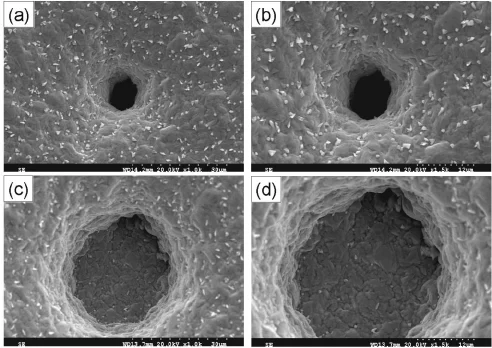
The core mechanism behind laser drilling microvias is ablation, where high-energy photons break molecular bonds in the target material, vaporizing it layer by layer. Laser parameters like wavelength, pulse duration, and fluence control the ablation depth and sidewall taper for optimal via geometry. In the microvia drilling process, the beam is scanned in patterns such as trepanning or helical drilling to form circular holes with minimal debris. Factories prioritize beam quality to achieve entrance and exit diameters within tight tolerances, ensuring reliable plating adhesion later. Thermal effects are managed by using short pulses to confine energy, preventing delamination in the surrounding laminate. This precision underpins the shift to HDI structures, where microvias stack across multiple layers without compromising structural integrity.
CO2 laser microvia drilling operates at wavelengths around 9.3 to 10.6 microns, excelling at ablating organic dielectrics like epoxy resins through thermal decomposition. The longer wavelength interacts strongly with carbon bonds, creating a clean cavity after copper foil removal. However, CO2 lasers produce a characteristic taper due to Gaussian beam profiles, which aids in plating but requires precise control to avoid resin smear. Factories often pair CO2 systems with desmear processes using plasma or permanganate to expose copper lands. This method suits blind vias from outer layers into inner cores, supporting build-up processes in HDI fabrication. Efficiency comes from high repetition rates, allowing rapid panel throughput in production environments.
UV laser microvia drilling employs shorter wavelengths, such as 355 nm from frequency-tripled Nd:YAG sources, enabling direct ablation of both copper and dielectrics. The photon energy exceeds copper's work function, facilitating photochemical bond breaking with less heat input compared to CO2 methods. This cold ablation process yields straighter sidewalls and smaller heat-affected zones, ideal for stacked microvias in advanced HDI. Copper drilling occurs first, followed by dielectric removal, often in a sequential or dual-laser setup for hybrid efficiency. Factories value UV lasers for their versatility across laminate types, including polyimides resistant to thermal damage. The result is higher aspect ratios and finer features, pushing the boundaries of interconnect density.
Laser ablation microvia formation integrates these principles by tailoring pulse overlap and energy density to material properties. Ablation thresholds vary; dielectrics require lower fluence than metals, guiding multi-step drilling sequences. Post-ablation, residue management ensures void-free electroplating, critical for via reliability under thermal cycling. Engineers model these interactions to predict taper angles and bottom roughness, informing design rules. In practice, ablation efficiency scales with laser power and optics, enabling sub-50 micron vias for next-generation boards. This foundational understanding drives consistent yields in high-volume manufacturing.
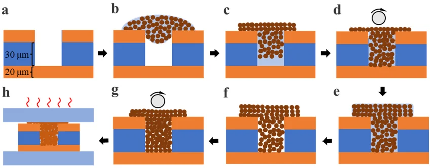
The Microvia Drilling Process in PCB Fabrication
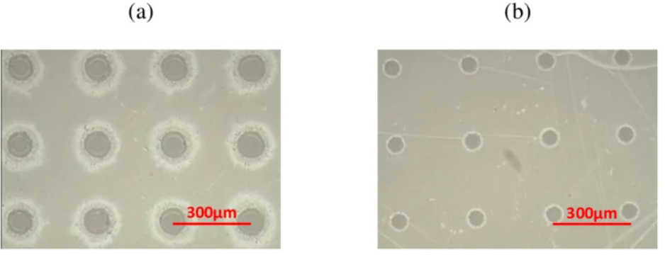
The microvia drilling process begins with panel preparation, including fiducial alignment for precise beam positioning on target lands. Outer copper is selectively etched or ablated to expose dielectric, preventing beam blockage and ensuring uniform energy delivery. Drilling follows in a controlled environment to minimize dust, with real-time monitoring of hole quality via inline optics. After ablation, desmear removes carbon residue and roughens walls for plating adhesion, typically via chemical or plasma methods. Sequential lamination builds additional layers, repeating the cycle for stacked vias. Final inspection verifies dimensions and continuity before full metallization.
In CO2 laser microvia workflows, panels are indexed under the galvo scanner, where pulses remove dielectric to the capture pad depth. Process parameters like pulse energy and repetition rate are optimized per material to balance speed and quality. Factories implement vision systems to detect defects like node cuts or icicle formations early. Transitioning to plating, the vias receive electroless seed and electroplated copper fill, often via moderate aspect ratio treat (MART) for reliability. This factory-driven sequence ensures compliance with design intents for HDI classes 2 through 4.
UV laser microvia processes shine in direct copper drilling, starting with low-fluence pulses to open foil without excessive melting. Dielectric ablation follows immediately, leveraging the beam's penetration for blind via formation. Hybrid systems alternate UV and CO2 passes for optimal results, enhancing throughput. Post-process cleaning addresses any haze or taper inconsistencies. Engineers appreciate the repeatability, as UV methods support tighter pitch arrays without mechanical wear.
Advantages of Laser Drilling Microvias: Precision and Efficiency
Laser drilling microvias offers unmatched precision for holes down to 50 microns, far surpassing mechanical drills limited by bit breakage and runout. Non-contact ablation eliminates burrs and stress cracks, preserving laminate integrity during high-volume production. Efficiency gains include drilling rates exceeding 1000 vias per second, reducing cycle times for HDI panels. Shorter signal paths from microvias improve electrical performance, with lower inductance aiding high-frequency signals. Factories report higher yields due to consistent hole geometries, minimizing scrap from via failures. Overall, this method scales seamlessly for complex builds like any-layer HDI.
Best Practices for Laser Drilling Microvias
Select laser-drillable dielectrics with low ablation thresholds and minimal charring, such as resin-coated copper or low-loss prepregs, to ensure clean via bottoms. Adhere to IPC-2226 guidelines for microvia placement, limiting stacks to three or four levels and staggering positions to avoid weak zones. Maintain outer copper at half-ounce weight to facilitate clean entry holes, reducing node cuts. Optimize laser parameters through test panels, targeting 0.8:1 aspect ratios for plating uniformity. Implement plasma desmear post-drilling to achieve surface roughness conducive to void-free fill. Regular calibration of beam delivery systems prevents drift, sustaining precision across production runs.
Quality control involves automated optical inspection for taper, diameter, and debris, followed by cross-section analysis on coupons. Reliability testing per IPC-6016 verifies microvia integrity under thermal shock and cycling. Factories track process windows to correlate parameters with failure modes like cracking. Design via-in-pad configurations with adequate annular rings for fanout. These practices, rooted in standard-aligned workflows, maximize first-pass yields.
Conclusion
Laser drilling microvias delivers precision and efficiency critical for advancing PCB fabrication in HDI applications. From CO2 and UV techniques to optimized processes, this method enables denser, reliable interconnects for electrical engineers. Factory insights emphasize material selection, parameter control, and standards compliance for success. As electronics miniaturize further, mastering the microvia drilling process will define fabrication capabilities. Integrating these principles ensures robust performance in demanding environments.
FAQs
Q1: What is the laser drilling microvia process?
A1: The laser drilling microvia process involves using focused beams to ablate copper and dielectric materials, forming blind vias under 150 microns. It starts with alignment, followed by sequential ablation, desmear, and plating. This non-contact method achieves high precision with minimal damage, ideal for HDI PCBs. Factories control parameters like pulse energy for consistent results across panels.
Q2: How does CO2 laser microvia differ from UV laser microvia?
A2: CO2 laser microvia excels at dielectric ablation via thermal processes at longer wavelengths, requiring prior copper removal. UV laser microvia handles both materials directly with cold ablation, yielding straighter walls. CO2 suits high-volume organic removal, while UV supports finer features. Selection depends on stackup and material for optimal efficiency.
Q3: What are best practices for laser ablation microvia in fabrication?
A3: Choose laser-drillable laminates and limit aspect ratios per IPC-2226 to ensure plating success. Use hybrid lasers for copper-dielectric combos and plasma desmear for clean walls. Inspect vias inline and test reliability via IPC-6016. Stagger stacks to prevent cracking, enhancing yield in production.
Q4: Why is precision important in the microvia drilling process?
A4: Precision in the microvia drilling process ensures reliable interconnections, minimizing voids and taper issues that cause failures. Tight tolerances support fine-pitch components and high-speed signals. It reduces layer count for compact designs while maintaining integrity under thermal stress.
References
IPC-T-50M — Terms and Definitions for Interconnecting and Packaging Electronic Circuits. IPC
IPC-2226 — Sectional Design Standard for High Density Interconnect (HDI). IPC
IPC-6016 — Qualification and Performance Specification for High Density Interconnect (HDI) Printed Boards. IPC