 ALLPCB


Introduction
Printed circuit board yield remains a critical performance metric in electronics manufacturing because every defective board increases material waste, rework costs, and delivery delays. Flying probe testing has emerged as a flexible, fixtureless method that verifies electrical integrity on bare boards and assembled units alike. By collecting detailed pass-fail and parametric data at each test point, manufacturers obtain the raw information needed for meaningful statistical analysis of defect patterns. This data-driven approach supports targeted process adjustments that raise overall first-pass yield without requiring large capital investments in dedicated test fixtures. When applied consistently, flying probe testing contributes directly to measurable improvements in PCB yield while aligning with established quality frameworks.
What Is Flying Probe Testing and Why It Matters
Flying probe testing uses multiple moving probes that travel across the board surface to contact designated test points in sequence. Unlike fixed-fixture methods, the system requires only CAD-derived test programs, allowing rapid changeovers between different board designs. The technique measures continuity, isolation, resistance, capacitance, and sometimes diode characteristics to detect opens, shorts, and incorrect component values. Because probes can access fine-pitch pads and high-density layouts that bed-of-nails fixtures often cannot reach, the method supports higher test coverage on complex boards. The resulting dataset of test outcomes provides the foundation for statistical evaluation of flying probe testing yield trends across production lots.
Technical Principles and Data Collection Mechanisms
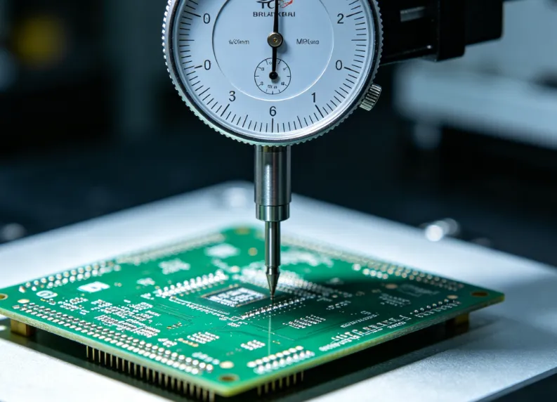
Each flying probe test cycle records the exact location, measured value, and pass-fail status for every net or component under test. These records accumulate into large datasets that reveal systematic defect distributions when analyzed over time. Common statistical tools include Pareto charts that rank defect types by frequency and control charts that track variation in measured parameters. Process capability indices calculated from the same data help quantify how well the manufacturing process meets specification limits. (Insert image: 'Flying Probe Tester in Operation' · ALT: 'Multiple flying probes contacting test points on a PCB panel') (Insert image: 'Defect Pareto Chart from Flying Probe Data' · ALT: 'Bar chart showing distribution of opens, shorts, and resistance failures')
Warpage and board flatness directly influence probe contact reliability and therefore affect measured yield. Excessive warpage can cause intermittent contact or false failures that inflate apparent defect rates.
Role of Industry Standards in Test Program Development
Test programs are developed with reference to IPC-A-600 for acceptability criteria and IPC-6012 for performance specifications of rigid boards. These documents define the visual and electrical thresholds that flying probe systems must verify. Adherence ensures that pass-fail decisions remain consistent across different production sites and over time. When test limits are set according to these standards, the collected statistics more accurately reflect true process capability rather than arbitrary tolerances.

Practical Best Practices for Yield Improvement
Effective implementation begins with thorough netlist verification and test-point optimization during the design-for-testability stage. Engineers review the test coverage report to confirm that critical nets receive adequate probing while avoiding redundant tests that extend cycle time. Production teams then run pilot lots and apply statistical process control to the flying probe results. When a particular defect category, such as opens on inner layers, shows elevated rates, root-cause analysis directs adjustments in drilling, plating, or lamination parameters. Regular review of flying probe testing statistics allows incremental refinements that compound into sustained yield gains.
Data integrity is maintained by calibrating probes at defined intervals and validating test programs against known-good boards. Outlier analysis helps distinguish genuine process issues from occasional probe wear or contamination. When these practices are followed, the statistical signals extracted from flying probe testing data become reliable indicators for continuous improvement initiatives.
Statistical Analysis of Yield Data
Yield improvement efforts rely on aggregating test results into lot-level metrics such as first-pass yield and defects per unit. Trend analysis over multiple lots identifies whether changes in material lots, equipment settings, or environmental conditions correlate with shifts in defect rates. Regression techniques can further explore relationships between measured parameters and final yield outcomes. Because flying probe systems generate point-specific data, engineers can map defects back to specific board regions or manufacturing steps, enabling precise corrective actions. Over successive production runs, these analytical steps typically produce a gradual upward trajectory in overall PCB yield.

Conclusion
Flying probe testing supplies detailed electrical data that supports rigorous statistical evaluation of PCB manufacturing performance. When programs are developed and maintained in accordance with IPC-A-600 and IPC-6012, the resulting statistics accurately reflect process health and guide effective yield-improvement actions. Consistent application of these methods reduces defect escape rates, lowers scrap, and improves delivery reliability for electrical engineering teams and their customers.
FAQs
Q1: How does flying probe testing improve PCB yield?
A1: Flying probe testing detects opens, shorts, and parametric deviations early in the production flow. The detailed data collected enables statistical identification of recurring defect patterns so that root causes can be addressed before they affect large volumes of boards. Over time, this targeted feedback loop raises first-pass yield and reduces the need for rework.
Q2: What statistical methods are commonly applied to flying probe testing data?
A2: Manufacturers use Pareto analysis to rank defect types, control charts to monitor process stability, and capability studies to quantify conformance to specifications. These techniques transform raw test records into actionable insights that support continuous yield improvement.
Q3: Can flying probe testing statistics reveal design-related yield issues?
A3: Yes. When defect locations cluster in specific board areas or net types, the data often points to design features such as insufficient spacing, marginal trace widths, or test-point accessibility problems. Engineers can then modify layouts or test programs to mitigate these issues in subsequent revisions.
Q4: How frequently should flying probe test programs be reviewed for yield optimization?
A4: Programs benefit from periodic review whenever new defect trends appear in the statistical reports or when design revisions are introduced. Regular calibration of the tester and validation against known-good samples further ensures that the collected data remains reliable for yield analysis.
References
IPC-A-600K — Acceptability of Printed Boards. IPC, 2020
IPC-6012E — Qualification and Performance Specification for Rigid Printed Boards. IPC, 2017
ISO 9001:2015 — Quality Management Systems. ISO, 2015


