 ALLPCB


Introduction
Surface Mount Technology, or SMT, plays a critical role in modern RF and microwave circuits by allowing compact component placement directly on the PCB surface. High-frequency applications demand precise implementation to maintain signal integrity and achieve proper impedance matching, as even minor deviations can lead to significant performance losses. Engineers increasingly rely on SMT for devices operating in GHz ranges, where miniaturization drives innovation in telecommunications, radar systems, and satellite communications. This article provides practical guidance on overcoming the unique challenges of SMT in RF and microwave environments, focusing on design, assembly, and troubleshooting strategies. By addressing these elements, teams can ensure reliable operation at microwave frequencies.
What Is SMT for RF and Microwave Applications and Why It Matters
SMT involves soldering components onto the surface of a printed circuit board without leads passing through holes, enabling higher component density and smaller form factors. In RF and microwave contexts, this technology supports frequencies from hundreds of MHz to tens of GHz, where traditional through-hole methods introduce excessive inductance and capacitance. Signal integrity becomes paramount, as high-frequency signals behave like transmission lines, susceptible to reflections from mismatches or discontinuities. Impedance matching ensures maximum power transfer and minimal losses, directly impacting system efficiency and noise figures. The shift to SMT matters because it aligns with the demand for cost-effective, high-performance boards in compact devices. Without proper SMT implementation, RF circuits risk degraded return loss, increased insertion loss, and electromagnetic interference.
Technical Principles Behind SMT in High-Frequency Environments
At microwave frequencies, electromagnetic waves interact strongly with PCB structures, turning traces into transmission lines governed by characteristic impedance. The skin effect confines currents to conductor surfaces, increasing effective resistance and necessitating wider traces or specialized finishes. Dielectric materials must exhibit low loss tangents to minimize signal attenuation, while substrate thickness affects both impedance and mechanical stability during reflow. Parasitic elements from SMT pads, such as pad capacitance and via stubs, can detune matching networks if not modeled accurately. Engineers must simulate these effects using field solvers to predict behavior before fabrication. Land pattern design per IPC-7351 standards helps mitigate parasitics by optimizing pad sizes and shapes for RF components.
Component leads in SMT introduce minimal inductance compared to through-hole, but fine-pitch RF passives and ICs require precise alignment to avoid solder bridges or voids. Thermal expansion mismatches between components and the board can cause warpage, exacerbating stress at high frequencies. Reflow soldering profiles must balance wetting and intermetallic formation to preserve surface finishes critical for low-loss connections. Signal propagation delays arise from group velocity variations in heterogeneous dielectrics, demanding uniform stackups. These principles underscore the need for integrated design and process control in SMT for microwave applications.
Practical Solutions and Best Practices for Implementation
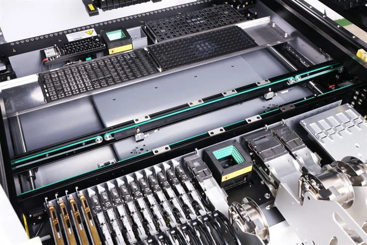
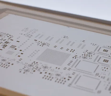
Start with PCB stackup design that supports 50-ohm or 75-ohm impedance traces, using coplanar waveguide or grounded coplanar structures for better field confinement. Select laminates with stable dielectric constants over frequency and temperature to maintain impedance matching across the operating band. Route high-frequency signals on outer layers to reduce dielectric losses, and use blind or buried vias for transitions to minimize stub effects. For SMT assembly, employ laser-cut stencils with apertures optimized for solder paste volume, ensuring uniform deposition on fine-pitch RF components. Precision pick-and-place machines with vision systems achieve sub-50-micron accuracy, vital for aligning microwave filters and amplifiers.
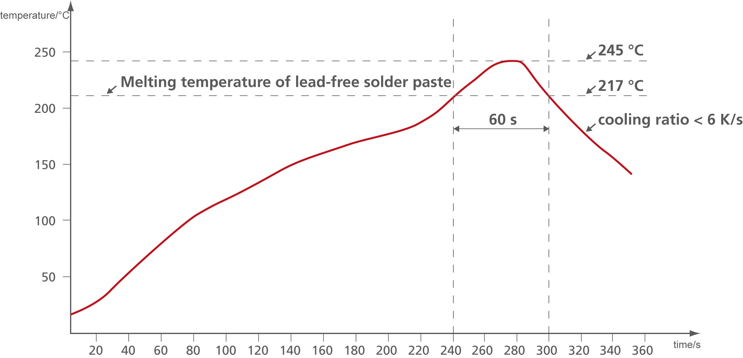
Reflow ovens should follow profiles that peak below component limits, with nitrogen atmospheres to prevent oxidation on exposed copper. Post-reflow inspection via automated optical systems verifies joint quality, focusing on voids that could alter RF performance. For signal integrity verification, integrate test points or connectors compatible with vector network analyzers to measure S-parameters early. Maintain cleanroom conditions to avoid contamination on sensitive RF surfaces. These practices, rooted in assembly expertise, reduce yield losses and enhance reliability.
Adherence to IPC-6018 qualification requirements ensures high-frequency boards withstand environmental stresses without delamination or dimension changes. J-STD-001 guidelines for soldering provide criteria for acceptable joints in high-reliability applications.
Troubleshooting Common Issues in SMT RF and Microwave Assemblies
One frequent problem is signal reflections due to impedance discontinuities at SMT pad transitions, manifesting as poor return loss above 10 GHz. Measure S11 parameters and adjust trace widths or add series capacitors to compensate. Solder voids under RF grounds create unintended cavities, acting as resonators; X-ray inspection identifies them, followed by targeted rework with low-temperature alloys. Component tombstoning occurs from uneven paste heating in fine-pitch passives, resolved by refining stencil thickness and reflow ramp rates. Warpage from CTE mismatches lifts edges during assembly, leading to open joints; counter this with symmetric stackups and fixture support.

Insertion loss spikes from conductor roughness or dielectric absorption require smoother copper foils and lower-loss materials. Simulate before build to isolate causes, then iterate prototypes. Electromagnetic coupling between adjacent traces degrades isolation; increase spacing or add ground planes. Overheating during reflow degrades RF transistor performance; profile ovens with thermocouples on test boards. Systematic troubleshooting, combining electrical tests and visual checks, restores functionality efficiently.
Conclusion
Implementing SMT for RF and microwave applications demands a holistic approach integrating design precision, material selection, and assembly rigor to safeguard signal integrity and impedance matching. Key practices like optimized land patterns, controlled reflow, and thorough testing mitigate high-frequency pitfalls effectively. Engineers benefit from standards-guided processes that ensure repeatability and performance. As frequencies rise, mastering these techniques positions teams for success in demanding applications. Prioritize simulation, validation, and iterative refinement for optimal results.
FAQs
Q1: What are the main challenges for signal integrity in SMT RF assemblies?
A1: High-frequency signals in SMT RF designs suffer from pad parasitics, via inductance, and dielectric losses that cause reflections and attenuation. Precise land patterns per industry standards minimize discontinuities, while short trace lengths reduce propagation delays. Controlled impedance routing and ground plane stitching preserve waveform integrity up to microwave bands. Regular S-parameter testing identifies issues early.
Q2: How does impedance matching impact SMT microwave performance?
A2: Impedance matching in SMT microwave circuits maximizes power transfer and minimizes VSWR, critical for amplifier stability and filter efficiency. Trace geometry, substrate properties, and component pads must align to 50 ohms typically. Discrepancies lead to standing waves and heat generation. Use field solvers during design and calibrate with TRL standards for verification.
Q3: Why is stencil design crucial for high-frequency SMT?
A3: Stencil apertures control solder paste volume, preventing bridges or insufficient joints in fine-pitch RF components that affect microwave signal paths. Trapezoidal walls improve release and uniformity at high speeds. Thinner foils, around 100 microns, suit 0.3mm pitches common in RF ICs. Validation through SPI ensures paste height consistency for reliable impedance.
Q4: What troubleshooting steps address reflow defects in RF SMT?
A4: Inspect for voids via X-ray, then adjust peak temperatures below 260C for sensitive components. Tombstoning fixes include slower preheat ramps for paste activation. Warped boards need fixturing; measure coplanarity pre-assembly. Electrical tests post-reflow confirm low insertion loss, guiding process tweaks.
References
IPC-6018D — Qualification and Performance Specification for High Frequency (Microwave) Printed Boards. IPC, 2020
IPC-7351C — Generic Requirements for Surface Mount Design and Land Pattern Standard. IPC, 2010
J-STD-001H — Requirements for Soldered Electrical and Electronic Assemblies. IPC, 2020


