ALLPCB


Introduction
High-frequency polyimide PCBs play a critical role in modern RF and microwave systems, where signal integrity and minimal losses are paramount. These boards leverage the unique properties of polyimide substrates to handle frequencies from hundreds of MHz up to tens of GHz. Engineers designing radar systems, satellite communications, and 5G infrastructure increasingly turn to polyimide for its thermal stability and electrical performance. Unlike standard FR-4 materials, polyimide maintains consistent characteristics under demanding conditions, making it ideal for optimizing performance in RF and microwave applications. This article explores the technical foundations, design considerations, and best practices for high-frequency polyimide PCBs. Readers will gain structured insights into achieving low signal distortion and high reliability.
What Are High-Frequency Polyimide PCBs and Why Do They Matter?
Polyimide PCBs use polyimide resin as the dielectric core, often in flexible or rigid-flex configurations suited for high-frequency operation. This material offers superior thermal endurance, withstanding temperatures beyond those tolerable by epoxy-based laminates. In RF and microwave contexts, polyimide's low moisture absorption prevents variations in electrical properties during environmental exposure. Its chemical resistance further enhances longevity in harsh operational settings. These attributes make polyimide a preferred choice over alternatives like PTFE for applications balancing flexibility and performance.
The relevance stems from the exponential increase in signal challenges at high frequencies. Polyimide addresses polyimide PCB signal loss by providing a stable platform for transmission lines such as microstrips and coplanar waveguides. In industries like aerospace and telecommunications, where downtime costs are high, these PCBs ensure reliable data transmission. Engineers value polyimide for enabling compact designs without compromising speed or integrity. As systems push toward mmWave bands, the demand for such materials grows, directly impacting project success.
Technical Principles of Polyimide in High-Frequency Applications
At the core of high-frequency polyimide PCB performance lies its dielectric properties. The high-frequency polyimide PCB dielectric constant remains low and stable across a broad frequency range, typically exhibiting values that support controlled impedance. This stability minimizes phase shifts and reflections in propagating signals. Polyimide's dissipation factor, a measure of energy loss per cycle, stays low, reducing attenuation in RF paths. Conductor losses from skin effect and dielectric losses from molecular polarization are both mitigated by the material's inherent characteristics. Radiation losses, though less dominant, are contained through proper grounding structures.
Signal propagation in polyimide follows transmission line theory, where characteristic impedance Z0 depends on substrate height, trace width, and dielectric constant. Variations in the high-frequency polyimide PCB dielectric constant with frequency or temperature can distort waveforms, but polyimide's consistency counters this. Polyimide PCB signal loss arises primarily from dielectric tangent and conductor resistance, both optimized in this material. At microwave frequencies, these losses compound, making material selection pivotal. Understanding these mechanisms allows engineers to predict and model performance accurately.
IPC-2221 provides guidelines for designing with such materials, emphasizing controlled impedance for high-speed signals. Thermal expansion mismatch between copper and polyimide requires careful layer sequencing to avoid delamination. Moisture ingress, though minimal, influences effective dielectric constant, underscoring the need for hermetic enclosures in some designs.
RF PCB Design Considerations for Polyimide Substrates
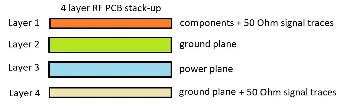
Effective RF PCB design considerations begin with stackup planning to achieve uniform dielectric thickness. Polyimide's flexibility aids in multilayer builds, but maintaining consistent core thickness controls the high-frequency polyimide PCB dielectric constant across the board. Trace routing prioritizes short paths for RF signals, avoiding bends sharper than 45 degrees to reduce reflections. Ground planes beneath transmission lines shield against crosstalk, a common issue at GHz frequencies. Vias introduce discontinuities; blind or buried types minimize stubs that cause resonances.
Impedance control is central, targeting 50 ohms for most RF lines using microstrip or stripline geometries. Polyimide PCB signal loss demands wider traces or thicker copper to counter skin effect losses, which scale with square root of frequency. Component placement groups RF sections away from digital noise sources, with stitching vias tying grounds. Thermal vias dissipate heat from active devices without altering RF paths. Simulation tools verify these layouts before fabrication.
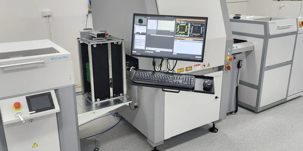
Fabrication tolerances tighten for high-frequency polyimide PCBs, per IPC-6012 standards for qualification. Etch factor influences trace geometry, impacting impedance by up to 10% if uncontrolled. Solder mask selection avoids high-loss dielectrics over RF traces.
Best Practices for Optimizing Polyimide PCB Performance
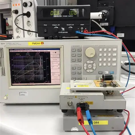
Select polyimide grades optimized for low dissipation factor to minimize polyimide PCB signal loss in microwave bands. Validate material datasheets for frequency-specific properties before design commitment. Employ symmetric stackups to balance warpage, critical for multilayer rigid-flex hybrids. During prototyping, measure insertion loss using vector network analyzers to correlate with simulations.
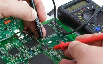
Assembly processes demand low-temperature soldering to preserve polyimide integrity, adhering to J-STD-020 for moisture sensitivity. Post-assembly testing includes time-domain reflectometry for impedance discontinuities. Environmental qualification simulates operational stresses, confirming stability.
Reliability enhances through via protection and conformal coatings, reducing corrosion risks. Documentation of RF PCB design considerations ensures repeatability across production runs.
Troubleshooting Common Issues in High-Frequency Polyimide PCBs
Excessive polyimide PCB signal loss often traces to inadequate ground return paths or via stubs. Inspect for delamination via cross-sectioning, especially after thermal cycling. Impedance mismatches manifest as S11 reflections; adjust trace widths iteratively. Warpage from CTE differences requires balanced copper distribution. Moisture-related shifts in high-frequency polyimide PCB dielectric constant resolve with bake-out prior to assembly.
Conclusion
High-frequency polyimide PCBs excel in RF and microwave applications through low, stable dielectric constants and minimal signal losses. Key RF PCB design considerations like stackup symmetry, precise routing, and impedance control unlock their potential. Adhering to standards such as IPC-2221 and IPC-6012 ensures manufacturability and reliability. Engineers benefit from polyimide's versatility in demanding environments, driving superior system performance. Future advancements will further refine these materials for emerging frequencies.
FAQs
Q1: What is the typical high-frequency polyimide PCB dielectric constant?
A1: Polyimide substrates offer a low and stable dielectric constant, often in the range of 3.4 to 3.6 at 1 GHz, making them suitable for RF transmission lines. This stability reduces phase distortion across microwave bands. Compared to FR-4, polyimide better maintains consistency with frequency changes.
Q2: How does polyimide PCB signal loss impact RF performance?
A2: Polyimide PCB signal loss primarily stems from low dissipation factors below 0.003, minimizing attenuation in high-frequency paths. This preserves signal amplitude for applications like radar. Poor design amplifies losses via reflections or crosstalk. Optimal trace geometry and grounding mitigate these effects effectively.
Q3: What are key RF PCB design considerations for polyimide materials?
A3: RF PCB design considerations include controlled impedance via precise stackup and trace widths, shielding with ground planes, and minimized via usage. Polyimide's thermal stability supports multilayer builds. Fabrication tolerances per IPC standards prevent variations. Simulation validates layouts pre-production.
Q4: Why choose polyimide for microwave PCBs over other materials?
A4: Polyimide provides flexibility, high thermal resistance, and low signal loss, ideal for compact microwave designs. Its chemical resistance suits harsh environments. Unlike rigid epoxies, it handles flexing without performance degradation. Stable properties ensure reliability in telecom and aerospace.