 ALLPCB


Introduction
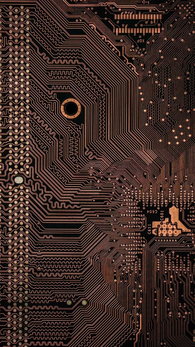
Printed circuit boards serve as the foundation for nearly all modern electronic devices, and the conductive traces that carry signals and power represent critical pathways whose integrity directly determines system reliability. When these traces sustain damage, engineers encounter intermittent failures, complete circuit outages, or gradual performance degradation that can prove difficult to isolate without systematic approaches. Effective diagnosis begins with understanding how trace damage manifests and what underlying mechanisms produce it. This guide provides structured methods for identifying root causes through logical inspection sequences and continuity verification techniques. Engineers benefit from applying these principles consistently across design reviews, manufacturing audits, and field troubleshooting scenarios.
Why Identifying PCB Trace Damage Matters for Electric Engineers
Trace damage disrupts the precise electrical paths that define circuit behavior, leading to signal integrity issues or power delivery failures that affect entire assemblies. In high-reliability applications such as industrial controls and medical instrumentation, undetected breaks or corrosion can escalate into costly downtime or safety concerns. Systematic diagnosis allows engineers to distinguish between trace-related faults and component-level problems, thereby streamlining repair workflows and reducing unnecessary part replacements. Industry standards such as IPC-6012E establish baseline expectations for trace quality during qualification, helping teams maintain consistent performance across production batches. Early identification also supports root-cause analysis that informs future design iterations and process improvements.
Common Mechanisms Leading to PCB Trace Breaks and Corrosion
Trace breaks often originate from mechanical stresses during handling, thermal cycling that induces expansion mismatches between copper and substrate materials, or manufacturing defects such as over-etching that thins conductor sections below acceptable limits. Corrosion develops when moisture and ionic contaminants combine with exposed copper surfaces, creating electrochemical reactions that progressively erode trace width and increase resistance. Thermal overstress from excessive current density accelerates these effects by generating localized heating that further weakens adhesion between copper and dielectric layers. Engineers evaluate these mechanisms by correlating observed failure patterns with environmental exposure histories and operating conditions. Structured analysis prevents misattribution of symptoms to unrelated factors such as solder joint degradation.
Observable Symptoms of PCB Trace Damage
Engineers typically first notice trace damage through symptoms such as intermittent connectivity during temperature changes, elevated voltage drops across specific board regions, or complete loss of signal paths in diagnostic testing. Visual indicators include discoloration along trace routes, lifted copper sections, or hairline fractures visible under magnification. In more advanced cases, corrosion produces powdery residues or pitting that alters trace geometry and increases susceptibility to further degradation. These symptoms align with acceptance criteria outlined in IPC-A-600K, which defines allowable limits for conductor defects and surface conditions. Documenting symptom patterns with photographs and measurement data enables reproducible diagnosis across multiple boards.
Practical Methods for Testing PCB Trace Continuity
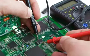
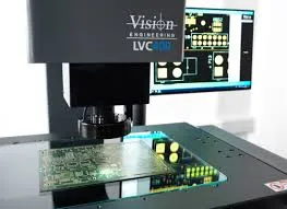
Continuity testing forms the core of any diagnostic protocol and begins with a calibrated multimeter set to low-resistance mode to detect open circuits or high-resistance segments along suspected traces. Engineers probe from endpoint pads or vias while systematically moving along the trace path to isolate the exact location of breaks. For complex boards, boundary-scan techniques or flying-probe systems provide automated mapping of continuity across dense interconnect networks. When corrosion is suspected, resistance measurements taken before and after gentle cleaning help quantify the extent of material loss. All testing procedures should follow documented sequences to ensure repeatability and avoid introducing additional damage during probing.
Related Reading: PCB Trace Repair for Beginners: A Hobbyist's Guide to Saving Damaged Boards
Structured Approach to Diagnosing Specific Trace Damage Types
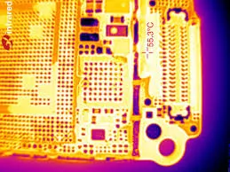
Begin diagnosis with a thorough visual examination under adequate lighting and magnification to identify obvious breaks, delamination, or surface corrosion. Next, perform continuity checks at multiple points to confirm electrical integrity and pinpoint discontinuity locations. When corrosion is indicated by elevated resistance or visual evidence, apply non-destructive cleaning methods followed by retesting to assess whether conductivity can be restored. Thermal imaging during low-power operation can reveal hot spots caused by narrowed trace sections carrying normal current loads. This layered approach ensures comprehensive coverage while minimizing the risk of overlooking secondary damage sites.
Best Practices for Accurate Root-Cause Identification
Engineers achieve reliable results by maintaining controlled environmental conditions during inspection to prevent moisture-related artifacts and by using calibrated instruments verified against known reference standards. Cross-verification between visual findings, electrical measurements, and historical operating data strengthens conclusions about whether damage stems from design, manufacturing, or field exposure. When standards such as IPC-A-600K are referenced during evaluation, teams maintain objective acceptance thresholds that reduce subjective interpretation. Regular training on updated inspection criteria and documentation of all diagnostic steps further supports consistent outcomes across engineering teams.
Related Reading: The Ultimate Guide to PCB Trace Repair: Step by Step for Engineers
Conclusion
Systematic diagnosis of PCB trace damage relies on combining visual inspection, continuity verification, and correlation with known failure mechanisms to isolate root causes effectively. Engineers who apply these logical sequences can distinguish between breaks, corrosion, and other degradation modes while adhering to established industry criteria. Consistent application of these methods supports faster resolution of field issues and contributes to improved long-term board reliability.
FAQs
Q1: How to find PCB trace damage during routine maintenance checks?
A1: Routine maintenance involves visual examination under magnification followed by continuity testing with a multimeter at multiple points along each trace. Engineers record resistance values and compare them against baseline measurements to detect gradual increases that signal developing breaks or corrosion. This process aligns with acceptance criteria in IPC-A-600K and helps identify issues before they cause system failures.
Q2: What are the main symptoms engineers should watch for when identifying PCB trace breaks?
A2: Common symptoms include intermittent signal loss, unexpected voltage drops, or complete open circuits detected during functional testing. Visual signs such as hairline fractures or discoloration along trace paths often accompany these electrical indications. Systematic probing confirms the location and extent of breaks.
Q3: How does diagnosing PCB trace corrosion differ from identifying mechanical breaks?
A3: Corrosion diagnosis requires checking for elevated resistance combined with visible surface degradation or residue, whereas mechanical breaks typically present as abrupt discontinuities without surface alteration. Engineers may perform cleaning and retesting to differentiate reversible corrosion effects from permanent material loss. Both conditions benefit from reference to IPC-6012E qualification requirements.
Q4: What techniques support effective testing of PCB trace continuity in dense layouts?
A4: Techniques include sequential multimeter probing from accessible pads, use of boundary-scan tools for automated mapping, and thermal imaging to locate high-resistance sections under load. These methods allow precise isolation of faults while preserving board integrity for further analysis.
References
IPC-6012E: Qualification and Performance Specification for Rigid Printed Boards.
IPC-A-600K: Acceptability of Printed Boards.


