 ALLPCB


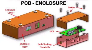
A precise fit between the PCB and its plastic enclosure is fundamental to product reliability. When dimensions or mounting points are misaligned, even a well-designed circuit can fail under stress or heat.
Many engineers encounter this issue not because of poor design skills, but because electrical and mechanical development happen in isolation. In today's compact and fast-paced electronic manufacturing, that gap is no longer acceptable.
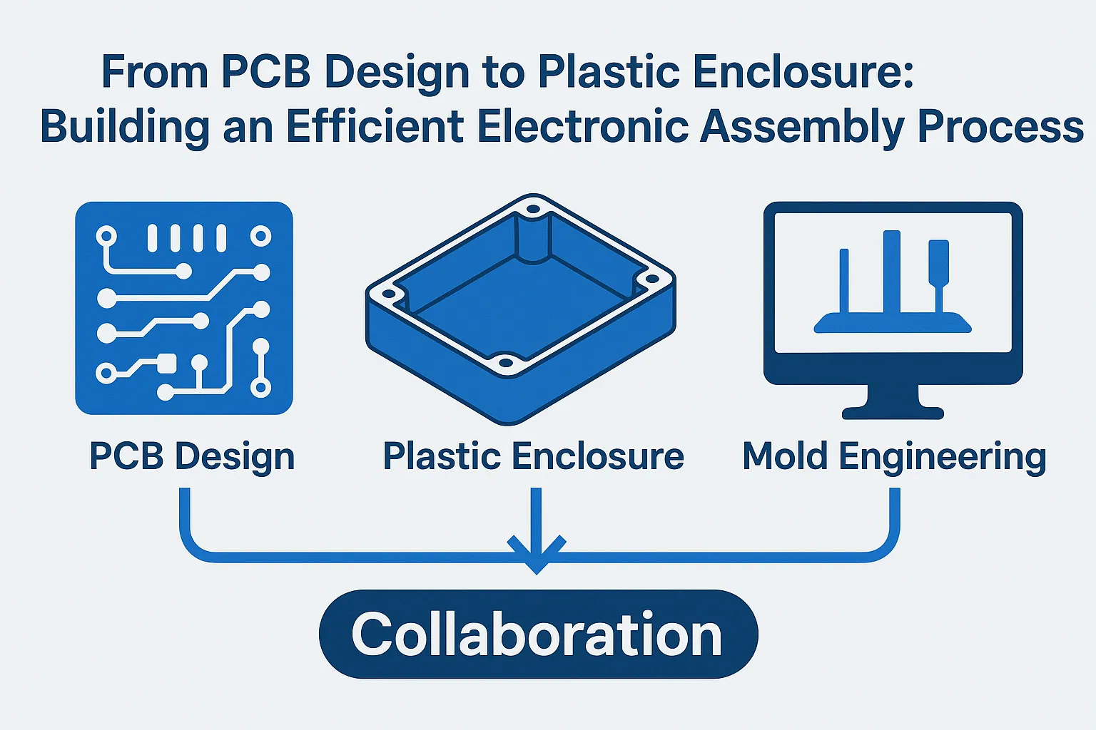
Ensuring collaboration between PCB layout, enclosure design, and mold engineering from the earliest stages leads to smoother assembly, fewer revisions, and a product that performs exactly as intended.
The Disconnect Between PCB and Enclosure Design
You've probably seen it happen before. The PCB is finalized. The enclosure tooling is approved. Everything looks perfect on paper — until the first assembled prototype arrives.
- Then something doesn't line up.
- A connector clashes with a wall.
- A mounting boss misses its hole by a millimeter.
- Airflow gets blocked where it matters most.
None of these are major design errors on their own, yet together they can delay a product launch by weeks.
When Teams Work in Isolation
These problems rarely stem from poor engineering — they come from disconnected workflows.
PCB designers operate in ECAD tools such as Altium or OrCAD, focusing on layout, routing, and signal integrity. Mechanical engineers, meanwhile, use 3D CAD platforms like SolidWorks or Creo to design enclosures and internal structures.
When these two domains evolve independently, mismatches become inevitable. The board outline may change after the enclosure model is complete, or the wall thickness might shift without anyone realizing how it affects the connector reach.
The Hidden Cost of Rework
The real cost isn't just rework — it's lost time. Each adjustment triggers a chain of updates:
- 3D model revisions
- Regenerated Gerber files
- New fit and function validation
In high-volume manufacturing, those delays ripple through tooling schedules and material procurement.
Bridging this gap requires more than data exchange — it demands synchronized decision-making. When the PCB and enclosure are treated as one integrated system, alignment issues disappear before they even begin.
Early Collaboration: The Foundation of a Reliable Assembly
Good assembly is built through early collaboration.
When PCB engineers, mechanical designers, and manufacturing partners exchange data early, small adjustments prevent major problems later.
You'd be surprised how often a five-minute discussion about connector spacing saves weeks of tooling modification.
Design for Manufacturability Starts Early
Early collaboration is the essence of Design for Manufacturability (DFM).
Instead of working in silos, share your PCB's 3D data with the enclosure team as soon as the layout stabilizes.
This allows mechanical engineers to:
- Visualize how mounting holes, ports, and heat zones align
- Check clearance, draft angles, and wall thickness
- Identify flow or warpage constraints before molding begins
At the same time, PCB designers gain feedback on mechanical limitations — creating a true two-way design process.
The Role of Modern ECAD–MCAD Integration
Modern tools make collaboration simple. Integrated platforms like Altium 365, Autodesk Fusion 360, or SolidWorks Electrical let teams view and modify the same model in real time.
You can:
- Check for interference automatically
- Run tolerance analyses
- Validate assembly methods before committing to tooling
When everyone works from the same digital source, misalignment becomes nearly impossible.
Why Mold Design Should Join the Conversation Early
Mold design also plays a vital role at this stage.
Parting lines, ejector pins, and gate positions can subtly affect how the enclosure interacts with the PCB after molding.
Involving a mold design specialist early ensures that enclosure geometry supports both manufacturability and long-term reliability. Aligning the mold's structural requirements with the PCB's geometry lays the foundation for a stable, scalable product.
Material and Process Selection: Where PCB Meets Plastic
When you design an electronic product, the PCB and enclosure never exist in isolation. They influence each other from the moment materials are chosen.
A mismatched pairing can create expansion gaps, warpage, or electrical noise — issues no amount of post-processing can fix.
Understanding Thermal Behavior
One of the biggest challenges lies in thermal behavior.
PCBs built on FR-4 or other laminates expand differently from molded plastics.
If the enclosure shrinks unevenly during cooling while the board expands under load, stress concentrates around screw bosses or solder joints. Over time, that stress leads to cracked housings or fatigued solder pads.
Choosing a resin with a thermal expansion rate that complements the PCB substrate is essential.
Balancing Heat Resistance and Safety
The enclosure must withstand soldering temperatures, internal heat, and external handling without deformation.
Flame-retardant plastics such as PC/ABS blends or UL-rated polycarbonate are common choices. They maintain mechanical stability, preserve clearance between circuits and housing, and prevent shorting under heat or vibration.
Designing for Molding Efficiency
The enclosure's geometry directly affects manufacturability.
To ensure consistent molding:
- Keep wall thickness uniform
- Use ribs for stiffness instead of thick walls
- Add sufficient draft angles for easy ejection
Ignoring these principles makes molding harder and affects how the PCB fits once inside. Even a small variation in wall thickness can distort connector alignment or strain mounting posts.
Why an Experienced Molding Partner Matters
A professional injection molding services provider translates design intent into production-ready geometry. They understand how resin flow, gate placement, and cooling channels influence dimensional accuracy.
By collaborating early with such partners, you ensure your PCB housing is both functional and repeatable — across thousands of production runs.
Material and process choices are never just about cost; they define product performance and scalability. When PCB and plastic meet under the same design logic, reliability becomes an engineered outcome.
Prototyping and Validation: Closing the Loop
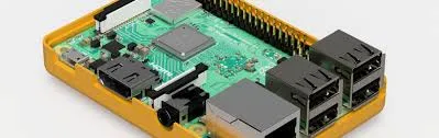
Even with perfect CAD data, confidence only comes after real-world validation. Virtual models show intent; physical prototypes reveal behavior. You need to see how the PCB slides into the enclosure, how the connectors align, and how the structure reacts under stress.
From Digital Design to Physical Insight
Rapid prototyping bridges that gap. Using 3D printing or CNC machining, you can produce housing samples within days instead of waiting for steel tooling.
These prototypes help you:
- Verify fit and clearance
- Validate standoffs, clips, and seals
- Observe tactile feel during insertion or fastening
Mounting the actual PCB lets you detect issues that no digital model could predict.
Testing Beyond Fit and Form
Mechanical fit is just the start. Early validation should also include:
- Thermal testing — how heat dissipates when the PCB is enclosed
- Vibration testing — to identify resonance that might loosen connectors
- Drop and impact testing — critical for handheld or portable products
Catching a clearance issue or weak latch during prototype testing is far cheaper than fixing it after the mold is cut.
The Economics of Early Validation
Fixing an interference issue in CAD might take hours; correcting it after tooling can take weeks — and cost thousands.
Rapid prototyping turns potential failures into controlled experiments. Each iteration confirms that electrical and mechanical design evolve together.
When your PCB supplier and enclosure manufacturer collaborate through this stage, iteration shifts from repair to refinement.
Case Study: When Design Alignment Changes Everything
Project Background
A small industrial IoT manufacturer was developing a compact sensor node — roughly the size of a matchbox. The PCB handled power regulation and signal processing, while the enclosure needed to withstand vibration and provide weather protection.
Initially, both teams worked independently. The PCB was finalized first; the enclosure came later.
It looked fine in CAD — until the first prototype revealed misaligned ports and an antenna positioned too close to the inner wall.
The enclosure had to be re-machined twice, delaying the project by nearly a month.
The Turning Point
After that setback, the company changed its workflow.
PCB and mechanical teams began sharing 3D data early. They used integrated ECAD–MCAD software to overlay the board and enclosure models and reviewed them jointly in weekly sessions.
The mold design partner was also involved early, advising on draft angles and gate placement before the enclosure was locked.
The difference was immediate. Connector positioning was verified in real-time, ventilation openings were optimized for heat flow, and moldability feedback ensured the wall thickness stayed uniform. No additional rework was needed during the next prototype round.
Measurable Outcomes:
- Rework time reduced by 70%, saving nearly three weeks in development.
- Tooling approval accelerated by 25%, since the mold model required no structural changes.
- Thermal performance improved by 15%, measured through enclosure temperature testing under continuous operation.
When PCB, enclosure, and molding experts began speaking the same design language, the process became faster, smoother, and more predictable.
Conclusion: Integration Is the Future of Electronic Manufacturing
When you step back and look at the entire design-to-production journey, one truth becomes clear — The days when PCB, enclosure, and mold design could operate in isolation are gone. Modern products are smaller, more complex, and expected to perform flawlessly straight off the assembly line. That only happens when electrical, mechanical, and manufacturing minds work as one.
When you share data, test together, and align design intent across disciplines, every component—from solder pad to screw boss—fits with purpose. The result is a product that assembles smoothly, scales efficiently, and meets its performance goals without compromise.


