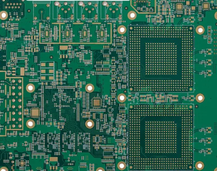
In the world of electronics, high-frequency PCB stack-up design is a critical factor for ensuring signal integrity and performance in modern devices. Whether you're working on telecommunications, automotive radar, or high-speed digital systems, a well-designed PCB stack-up can make or break your project. This guide dives deep into the essentials of high-frequency PCB layer stack design, covering topics like impedance control, microstrip vs. stripline configurations, multilayer setups, and the importance of ground planes. Let's explore how to optimize your PCB for high-frequency applications with practical tips and detailed insights.
What Is High-Frequency PCB Stack-Up Design?
A PCB stack-up refers to the arrangement of copper layers and insulating materials (dielectrics) in a printed circuit board. For high-frequency applications—typically involving signals above 100 MHz—the stack-up design becomes crucial. These designs must minimize signal loss, control impedance, and reduce electromagnetic interference (EMI). A proper high-frequency PCB layer stack ensures that signals travel efficiently without distortion, crosstalk, or unwanted noise.
In this comprehensive guide, we'll break down the key elements of designing a stack-up for high-frequency circuits, providing actionable advice for engineers and designers looking to optimize their boards.
Why High-Frequency PCB Stack-Up Design Matters
High-frequency signals are sensitive to the physical properties of a PCB. Factors like trace width, dielectric thickness, and layer arrangement directly impact signal speed and integrity. A poorly designed stack-up can lead to issues such as:
- Signal reflections due to impedance mismatches.
- Increased crosstalk between adjacent traces.
- Higher EMI, which can interfere with nearby components or systems.
- Signal loss due to dielectric materials unsuitable for high frequencies.
By carefully planning the high-frequency PCB layer stack, you can avoid these problems and ensure reliable performance in applications like 5G, RF systems, and high-speed data transfer.
Key Considerations for High-Frequency PCB Stack-Up Design
1. Layer Count and Arrangement
The number of layers in a PCB depends on the complexity of the circuit and the need for signal isolation. For high-frequency designs, multilayer boards (4 layers or more) are common. A typical 4-layer stack-up might look like this:
- Top Layer: Signal traces (often microstrip).
- Layer 2: Ground plane for shielding and return paths.
- Layer 3: Power plane or additional ground.
- Bottom Layer: Signal traces or additional components.
For more complex designs, 6- or 8-layer boards provide extra space for dedicated signal layers and additional ground planes, improving isolation and reducing noise. When arranging layers, always place signal layers adjacent to ground planes to create a controlled impedance environment.
2. Material Selection for High-Frequency Applications
The dielectric material between layers plays a huge role in high-frequency performance. Standard FR-4 materials, with a dielectric constant (Dk) of around 4.2-4.5, may not be ideal for frequencies above 1 GHz due to higher signal loss. Instead, consider low-loss materials like:
- Rogers RO4350B (Dk ≈ 3.48, low loss tangent of 0.0037 at 10 GHz).
- Isola IS680 (Dk ≈ 3.0, designed for high-speed and RF applications).
- Teflon-based materials for ultra-high-frequency designs.
Choosing the right material reduces signal attenuation and ensures consistent impedance across frequencies.
3. PCB Stackup Impedance Control
Impedance control is a cornerstone of high-frequency PCB design. Uncontrolled impedance can cause signal reflections, degrading performance. For high-frequency signals, common impedance targets are 50 ohms (for RF) or 100 ohms differential (for high-speed digital signals).
To achieve PCB stackup impedance control, consider the following:
- Trace Width and Spacing: Use impedance calculators to determine the correct trace width for your target impedance. For a 50-ohm microstrip on a 4-layer board with a 1.6mm thickness and FR-4 dielectric, the trace width might be around 0.3mm.
- Dielectric Thickness: The distance between a signal layer and its reference plane (ground or power) affects impedance. Thinner dielectrics result in lower impedance for the same trace width.
- Reference Planes: Ensure signal traces are routed over continuous ground or power planes to maintain consistent impedance.
Many design tools include built-in impedance calculators to help you fine-tune your stack-up for specific values.
Microstrip vs. Stripline in High-Frequency PCB Design
When routing high-frequency signals, two common transmission line structures are used: microstrip and stripline. Understanding the differences in microstrip vs. stripline high-frequency applications is key to choosing the right configuration for your stack-up.
Microstrip: Surface-Level Traces
Microstrip traces are placed on the outer layers of a PCB, with a ground plane directly below. They are easier to fabricate and inspect, making them a popular choice for many designs.
- Advantages: Simple to design, lower cost, and accessible for rework or testing.
- Disadvantages: More susceptible to EMI since they are exposed on the surface. Signal loss can also be higher due to radiation effects at very high frequencies (above 5 GHz).
- Best Use: Moderate high-frequency applications (up to a few GHz) where cost is a concern.
Stripline: Embedded Traces
Stripline traces are sandwiched between two ground planes within the PCB, offering better shielding and reduced EMI.
- Advantages: Superior EMI protection and lower radiation loss, making them ideal for ultra-high-frequency signals (above 5 GHz).
- Disadvantages: More complex to design and manufacture, as they require precise dielectric thickness control. Harder to access for testing or modifications.
- Best Use: High-frequency RF designs where signal integrity and EMI reduction are critical.
For most high-frequency applications, a combination of both structures might be used. Microstrip can handle less sensitive signals on outer layers, while stripline protects critical signals inside the board.
Designing a Multilayer PCB for High-Frequency Signals
In multilayer PCB design, the stack-up becomes even more complex as you add layers for additional signals, power, and ground planes. A well-designed multilayer board balances signal integrity with manufacturability. Here are some best practices:
- Symmetry: Keep the stack-up symmetrical to avoid warping during manufacturing. For an 8-layer board, pair signal and plane layers evenly on both sides of the center.
- Signal Layer Placement: Place high-speed or high-frequency signal layers close to ground planes to control impedance and reduce crosstalk.
- Power and Ground Planes: Dedicate internal layers to power and ground to provide stable voltage distribution and low-inductance return paths for signals.
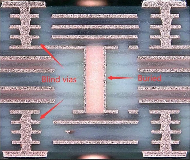
- Via Management: Minimize the use of vias for high-frequency signals, as they introduce inductance and can disrupt impedance. When necessary, use back-drilling to remove unused via stubs.
For example, an 8-layer high-frequency stack-up might be arranged as:
- Top Signal (Microstrip)
- Ground Plane
- Signal Layer (Stripline)
- Power Plane
- Ground Plane
- Signal Layer (Stripline)
- Ground Plane
- Bottom Signal (Microstrip)
This configuration ensures that each signal layer has a nearby reference plane for impedance control and shielding.
The Role of Ground Planes in High-Frequency Stack-Ups
A solid ground plane stackup high-frequency design is essential for maintaining signal integrity. Ground planes serve multiple purposes:
- Return Path: High-frequency signals need a low-inductance return path. A continuous ground plane beneath signal traces ensures minimal loop inductance.
- Shielding: Ground planes reduce crosstalk and EMI by isolating signals on different layers.
- Impedance Control: The proximity of a ground plane to a signal trace determines the characteristic impedance, which must be consistent for high-frequency performance.
Always avoid splitting ground planes under high-frequency traces, as this can disrupt the return path and cause signal reflections. If multiple ground planes are used, connect them with vias at regular intervals to maintain a uniform reference.
Practical Tips for High-Frequency PCB Stack-Up Design
Here are some actionable tips to refine your high-frequency PCB stack-up:
- Use Simulation Tools: Before finalizing your design, simulate the stack-up using tools to predict impedance, signal loss, and EMI behavior.
- Minimize Layer Transitions: Keep high-frequency signals on a single layer when possible to avoid impedance discontinuities caused by vias.
- Control Dielectric Thickness: Work closely with your manufacturer to ensure precise dielectric thickness, as even small variations can affect impedance.
- Test Prototypes: Build and test prototypes to validate your stack-up design under real-world conditions, especially for frequencies above 1 GHz.
Common Challenges and How to Overcome Them
Designing a high-frequency PCB stack-up comes with challenges. Here are a few common issues and solutions:
- Signal Loss: Use low-loss dielectric materials and keep trace lengths short to minimize attenuation.
- Crosstalk: Increase spacing between high-frequency traces and use ground planes or guard traces for isolation.
- Manufacturing Tolerances: Account for variations in trace width and dielectric thickness during design by adding margins to impedance calculations.
Conclusion: Mastering High-Frequency PCB Stack-Up Design
Creating an effective high-frequency PCB layer stack is both an art and a science. By focusing on PCB stackup impedance control, choosing between microstrip vs. stripline high-frequency configurations, optimizing multilayer PCB design, and prioritizing a robust ground plane stackup high-frequency setup, you can ensure your board performs flawlessly even at the highest frequencies.
Start with a clear understanding of your signal requirements, select the right materials, and use precise design techniques to build a stack-up that supports your application. With the insights and tips shared in this guide, you're well-equipped to tackle the challenges of high-frequency PCB design and deliver reliable, high-performance boards for any project.
 ALLPCB


