ALLPCB


Introduction
In multilayer FR-4 PCB design, the layer stackup serves as the foundation for reliable performance, particularly in high-speed and high-density applications favored by electric engineers. Proper stackup configuration ensures controlled impedance, minimal crosstalk, and efficient power distribution while mitigating issues like warpage and thermal stress. FR-4, a widely used glass-reinforced epoxy laminate, offers cost-effective mechanical stability and electrical properties suitable for most commercial electronics. However, optimizing the stackup requires adherence to established engineering principles to balance signal integrity with manufacturability. This article explores FR-4 PCB layer stackup rules, impedance control strategies, power and ground plane design, and signal layer routing techniques. Engineers can apply these best practices to enhance PCB reliability and performance in complex designs.
Understanding FR-4 PCB Layer Stackup and Its Importance
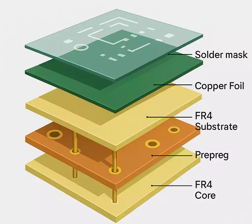
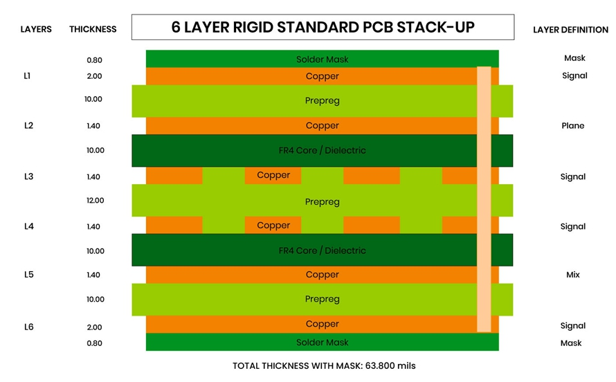
FR-4 PCB layer stackup refers to the sequential arrangement of copper conductive layers, dielectric cores, and prepregs that form the board's vertical structure. Each layer contributes to signal propagation, power delivery, and mechanical integrity, making stackup design a critical step in the PCB development process. In multilayer FR-4 PCB design, improper stackup can lead to signal distortion, increased EMI, or board deformation during fabrication or operation. For electric engineers working on dense interconnects, stackup directly impacts impedance matching and return path efficiency, which are essential for high-frequency signals. Why does it matter? Poor stackup choices amplify losses in data transmission rates and complicate impedance control, potentially requiring costly respins. Adhering to FR-4 PCB layer stackup rules early prevents these pitfalls and aligns with industry expectations for robust designs.
The relevance extends to thermal management, as FR-4's coefficient of thermal expansion influences layer adhesion under soldering temperatures. Engineers must consider core and prepreg thicknesses to maintain planarity and avoid via barrel cracks. Stackup optimization also supports power integrity by positioning planes strategically for low-inductance paths. In practice, a well-defined stackup reduces design iterations and accelerates time-to-market for electric systems.
Core Technical Principles of FR-4 Layer Stackup
The dielectric properties of FR-4, including its relative permittivity around 4.0 to 4.7, govern signal propagation speeds and characteristic impedance in multilayer configurations. In FR-4 PCB impedance control stackup, engineers calculate impedance using transmission line models for microstrip and stripline geometries, factoring in copper thickness, dielectric height, and etch factors. Symmetry in the stackup is paramount to counteract warpage from asymmetric copper distribution, which arises due to differing CTEs between copper and FR-4. Core principles include alternating signal and plane layers to provide low-impedance return paths, minimizing loop inductance. Adherence to IPC-2221 guidelines ensures these principles translate to manufacturable designs with predictable electrical behavior.
Another key mechanism involves plane capacitance formed between adjacent power and ground layers, which acts as a distributed decoupling reservoir. In FR-4 PCB power and ground plane design, thin dielectrics between planes increase capacitance density, aiding high-frequency noise suppression. Signal layers benefit from embedding between planes to shield against external interference, a concept central to controlled impedance. Thermal conductivity through the stackup affects heat dissipation, with via stitching enhancing plane-to-plane thermal coupling. Engineers must model these interactions to predict performance under operational stresses.
FR-4 PCB Layer Stackup Rules for Reliable Designs
FR-4 PCB layer stackup rules emphasize balanced copper weight distribution to prevent bow and twist during lamination. For even-layer counts like 4 or 6, place signal layers externally with internal planes for symmetry, while odd-layer boards require a hybrid outer plane. Minimum dielectric thicknesses should accommodate fabrication tolerances, typically starting from standard core and prepreg combinations. Avoid placing high-current traces adjacent to sensitive signals without ground shielding to reduce crosstalk. These rules, rooted in standard design practices, ensure mechanical stability and electrical isolation.
Layer pairing is crucial: pair high-speed signals with nearby reference planes to control impedance and provide return currents. In multilayer FR-4 PCB design, limit signal layers to those immediately adjacent to planes, reserving outer layers for low-speed or power routing where possible. Via aspect ratios must stay below 10:1 to maintain plating integrity, influencing stackup thickness choices. Engineers should prioritize uniform prepreg fill in blind vias for consistent dielectric properties. Following these FR-4 PCB layer stackup rules minimizes field fringing and supports high-yield production.
Achieving Impedance Control in FR-4 PCB Stackups
FR-4 PCB impedance control stackup relies on precise dielectric spacing and material uniformity to achieve target values like 50 ohms single-ended or 100 ohms differential. Microstrip lines on outer layers exhibit higher impedance due to air exposure, while striplines embedded in FR-4 offer tighter control with dual reference planes. Engineers adjust trace width and dielectric thickness iteratively, accounting for etch-back and copper foil roughness. Tolerance stacking from prepreg variations necessitates statistical modeling for production yields. Consistent resin content in FR-4 prepregs is vital for repeatable Dk values across the panel.
For differential pairs, symmetric spacing to ground planes prevents skew and common-mode noise. In high-layer-count stackups, plane splits must be distant from signal vias to avoid impedance discontinuities. IPC-6012 specifications guide qualification of these controlled-impedance boards through cross-section analysis. Optimization involves trade-offs between line width feasibility and routing density. Electric engineers benefit from stackup previews in design flows to validate impedance pre-layout.
Optimizing FR-4 PCB Power and Ground Plane Design
FR-4 PCB power and ground plane design focuses on minimizing voltage droop and EMI through solid, unbroken planes spanning the board area. Position ground planes adjacent to every signal layer to form tight coupled pairs, reducing inductance to picohenry levels per square. Power planes should interleave with grounds, using thin core dielectrics for higher decoupling capacitance. Stitching vias along plane edges and splits provide current return paths and shield signals. These practices enhance power integrity in dense multilayer FR-4 PCB design.
Plane voltage domains require careful segmentation to isolate noise, with overlap regions featuring stitching capacitors. Thermal relief patterns on vias prevent solder joint cracks while maintaining low resistance. In high-power applications, thicker copper or multiple plane layers distribute current evenly. Engineers must simulate PDN impedance to verify margins against ripple specifications. Ground plane integrity directly supports FR-4 PCB signal layer routing by providing clean references.
Best Practices for FR-4 PCB Signal Layer Routing in Multilayer Designs
FR-4 PCB signal layer routing demands adherence to length-matching for clocks and data pairs, minimizing skew in high-speed interfaces. Route critical signals as straight as possible on dedicated layers, avoiding bends sharper than 3:1 width-to-length ratios to preserve impedance. In multilayer FR-4 PCB design, length-tune serpentine patterns on inner layers reduce radiation compared to outer routing. Broadside coupling between adjacent signal layers should be minimized through plane shielding. These techniques align with FR-4 PCB layer stackup rules for optimal integrity.
Use blind or buried vias for dense routing to shorten stub lengths, preserving signal quality. Fanout patterns from BGA packages require staggered grids with ground vias interleaved. Engineers should allocate layers by speed: fastest signals inner-most for best shielding. Post-routing verification checks for violations like unmatched lengths or excessive vias. Practical implementation yields robust, high-performance boards.
Common Challenges and Troubleshooting in Stackup Optimization
Engineers often encounter warpage in asymmetric stackups, addressed by adding dummy copper pours or balancing with non-functional planes. Impedance deviations arise from prepreg flow inconsistencies, mitigated by specifying low-flow materials for tight stacks. Power plane resonance can couple noise to signals, resolved by strategic capacitor placement and plane partitioning. Via transitions in high-layer counts introduce stubs; back-drilling offers a solution where feasible. Troubleshooting involves cross-section microscopy per IPC-A-600 criteria to validate layer alignment and plating.
Thermal cycling stresses test stackup robustness, revealing delamination risks from CTE mismatch. Simulations predict these failures, guiding iterative refinements. Collaborative reviews between design and fabrication teams ensure stackup feasibility.
Conclusion
Mastering FR-4 PCB layer stackup design integrates FR-4 PCB layer stackup rules, precise impedance control, effective power and ground plane design, and disciplined signal layer routing. These best practices enable electric engineers to deliver high-reliability multilayer FR-4 PCB designs with superior signal and power integrity. Symmetry, coupling, and standardization form the core of optimization, reducing risks in fabrication and operation. By applying these structured approaches, teams achieve efficient, performant boards aligned with industry benchmarks. Future designs will leverage advancing simulation for even tighter margins.
FAQs
Q1: What are the key FR-4 PCB layer stackup rules for preventing warpage?
A1: FR-4 PCB layer stackup rules prioritize symmetric copper distribution by alternating signal and plane layers evenly through the thickness. Use balanced core and prepreg thicknesses to match CTE across the build. Avoid heavy outer-layer copper without internal counterparts. These steps minimize bow and twist during lamination and reflow, ensuring flatness for assembly. Engineers verify symmetry via simulation and cross-sections.
Q2: How does FR-4 PCB impedance control stackup affect high-speed signals?
A2: FR-4 PCB impedance control stackup defines trace geometry relative to reference planes, controlling propagation delay and reflections. Embed high-speed lines in striplines for stable 50-ohm impedance with minimal variation. Adjust dielectric spacing and widths for differential pairs to match common 100-ohm targets. This setup reduces crosstalk and maintains eye diagram integrity in gigabit applications. Validation through TDR testing confirms compliance.
Q3: What considerations apply to FR-4 PCB power and ground plane design in multilayer boards?
A3: In FR-4 PCB power and ground plane design, place planes adjacent to signals for low-inductance returns and decoupling. Use thin dielectrics between planes to boost capacitance and filter noise. Segment power domains with stitching vias at edges to contain fields. This multilayer FR-4 PCB design approach supports clean power delivery and EMI suppression. Simulations verify PDN performance pre-fabrication.
Q4: Why is signal layer routing critical in multilayer FR-4 PCB design?
A4: FR-4 PCB signal layer routing in multilayer FR-4 PCB design requires plane-proximate paths for controlled impedance and shielding. Length-match pairs to avoid skew, using broadside avoidance on adjacent layers. Buried vias shorten paths, minimizing stubs. These practices preserve signal quality amid density demands. Routing reviews ensure adherence to stackup intent.