 ALLPCB


Introduction
Flexible printed circuit boards, commonly known as flex PCBs, enable innovative designs in space-constrained and mechanically demanding applications. These circuits conform to irregular shapes, tolerate repeated bending, and integrate seamlessly into products like consumer electronics, aerospace systems, and medical implants. For electric engineers working with a flex PCB manufacturer, mastering design considerations ensures optimal performance and longevity. Key factors include flexible PCB design rules, material choices, and bend radius specifications tailored to static or dynamic use. This article delves into these elements, offering factory-driven insights aligned with industry standards to guide your manufacturing process. By following best practices, engineers can minimize failures and achieve reliable production outcomes.
What Are Flex PCBs and Why They Matter
Flex PCBs consist of thin, bendable substrates that replace rigid boards in applications requiring flexibility or minimal weight. Unlike rigid PCBs, they use polyimide or polyester films as base materials, allowing circuits to flex without fracturing. This capability matters in industries where components must endure vibration, thermal cycling, or tight packaging, such as in smartphones, sensors, and robotics. Poor design leads to issues like trace cracking or delamination during manufacturing or operation, increasing costs and delays. Engineers must prioritize flexible PCB design rules from the outset to balance electrical performance with mechanical durability. As demand grows for compact devices, flex PCBs represent a critical evolution in interconnect technology.

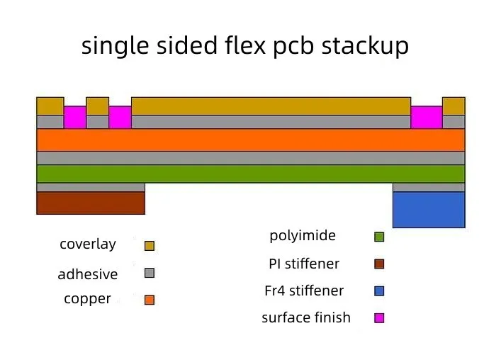
Flex PCB Materials: Selection and Properties
Flex PCB materials form the foundation of reliable manufacturing, with polyimide dominating due to its high thermal stability and flexibility. These films offer excellent tensile strength, low moisture absorption, and resistance to chemicals encountered in assembly processes. Adhesiveless laminates enhance signal integrity by reducing interfaces prone to peeling. Copper foil types, such as rolled annealed or electrodeposited, influence bend performance; rolled annealed copper excels in dynamic applications for its grain structure that resists cracking. Coverlays protect traces while maintaining flexibility, typically using polyimide with adhesive layers. Material selection must align with environmental exposures, ensuring compatibility throughout the production cycle.
When choosing flex PCB materials, consider dielectric constants for high-frequency signals and CTE matching to prevent stress at interfaces. Factory processes like lamination and etching demand materials that withstand elevated temperatures without warping. IPC-6013 provides qualification criteria for these substrates, specifying tests for adhesion and flexibility. Engineers should request material datasheets verifying compliance to avoid variability in yields. Proper selection reduces defects like cracking during flexing or voids in vias.
Key Flexible PCB Design Rules
Flexible PCB design rules dictate trace geometry, spacing, and pad sizes to prevent failures under mechanical stress. Minimum trace widths typically start at 75 microns for high-density designs, with spacing adjusted for voltage and manufacturing tolerances. Vias require staggered placement to distribute strain, avoiding inline arrays that concentrate bends. Hole sizes must exceed 0.3 mm to facilitate plating without barrel cracking. Annular rings around pads should measure at least 0.15 mm to accommodate etch factors. These rules ensure manufacturability while preserving electrical isolation.
Layer stackups demand careful planning, with signal layers separated by flex cores and stiffeners added for connector mounting. Dynamic flex PCB designs incorporate wider traces in bend zones to handle strain. IPC-2223 outlines sectional standards for stackup configurations, emphasizing bend area reinforcements. Avoiding sharp corners in traces prevents fatigue points, favoring teardrop entries for pads. Engineers benefit from simulating strain distribution early to refine rules iteratively.
Bend Radius Flex PCB: Critical Specifications
The bend radius flex PCB parameter defines the tightest curve a circuit can endure without damage, directly impacting design feasibility. Static bends allow tighter radii, often 10 times the total thickness, while dynamic applications require 100 times or more to prevent copper fatigue. Total thickness includes substrate, copper, and coverlay, so thinner constructions enable sharper bends. Factory testing verifies compliance through cyclic flexure, measuring cycles to failure. Exceeding minimum radii risks microcracks propagating under thermal expansion.
Mandrel bend tests simulate real-world use, with inner radius measured against outer foil strain. For dynamic flex PCB, engineers specify minimum dynamic bend radii based on cycle counts, often 20-50 times thickness for millions of cycles. Material ductility influences this; polyimide with RA copper supports tighter radii than polyester. Design software flags violations, but validation via prototypes confirms rules. Consistent bend radius control during manufacturing prevents field failures in moving assemblies.
Designing Dynamic Flex PCBs
Dynamic flex PCB applications, like hinges in laptops or robotic joints, demand reinforced bend zones with patterned copper to relieve stress. These zones use hatched or slotted traces, reducing material in high-strain areas while maintaining conductivity. Stiffeners localize rigidity at terminations, transitioning smoothly to flex regions. Coverlay openings over connectors ease strain during mating. Multilayer dynamic designs incorporate floating ground planes to shield signals amid movement.
Thermal management poses challenges, as flexing exacerbates CTE mismatches leading to delamination. Engineers mitigate this with balanced stackups and low-CTE adhesives. J-STD-001 guidelines influence assembly tolerances for dynamic boards, ensuring solder joints withstand flex cycles. Prototyping with accelerated life testing reveals weaknesses early. Factory insights emphasize tooling for precise registration in dynamic zones, avoiding misalignment that amplifies strain.
Manufacturing Best Practices for Flex PCBs
Adhering to manufacturing best practices starts with panelization strategies that minimize waste and stress during depanelization. Laser routing preserves edges over shearing, reducing microcracks. Etching processes use controlled sprays to maintain trace fidelity in fine features. Lamination under vacuum prevents air entrapment, crucial for multilayer flex. Post-processing includes plasma cleaning for adhesion before coverlay application.
Quality control involves 100% electrical testing and cross-section analysis for plating thickness. Solder mask alternatives like photoimageable coverlays offer finer resolution. For dynamic flex PCB, endurance testing per IPC-6013 verifies cycle life. Traceability from design to shipment ensures repeatability. Partnering with a flex PCB manufacturer experienced in these practices yields higher first-pass yields and reliability.
Handling during shipping uses rigid carriers to prevent unintended bends. Environmental controls in the factory maintain humidity below 60% to avoid hygroscopic issues. Final inspections check for warpage under IPC-A-600 criteria, ensuring flatness for assembly.
Conclusion
Flex PCB manufacturing hinges on integrating flexible PCB design rules, appropriate flex PCB materials, precise bend radius flex PCB specs, and robust processes for dynamic applications. Engineers who prioritize these elements achieve durable, high-performance circuits suited to demanding environments. Standards like IPC-2223 and IPC-6013 provide the framework for success, guiding from concept to production. By applying these best practices, teams reduce risks, optimize costs, and accelerate time-to-market. As flex technology advances, staying aligned with factory insights will drive innovation in compact electronics.
FAQs
Q1: What are the essential flexible PCB design rules for manufacturing?
A1: Flexible PCB design rules focus on trace width, spacing, via placement, and annular rings to withstand bending stresses. Minimum widths of 75 microns and staggered vias prevent cracking in bend zones. Stackups must balance layers for strain distribution, with IPC-2223 providing sectional guidelines. Engineers should simulate designs and prototype to validate rules, ensuring compatibility with flex PCB manufacturer capabilities. These rules enhance yield and reliability.
Q2: How do I select flex PCB materials for dynamic applications?
A2: Choose polyimide films with rolled annealed copper for superior ductility in dynamic flex PCB use. Adhesiveless laminates minimize peel risks under repeated cycles. Verify thermal stability and CTE via datasheets aligned with IPC-6013 specs. Thinner substrates enable tighter bend radii while maintaining signal integrity. Factory testing confirms material performance before full production.
Q3: What is the importance of bend radius flex PCB in design?
A3: Bend radius flex PCB specs determine the minimum curve without damage, critical for static or dynamic use. Static allows 10x thickness, dynamic up to 100x for longevity. Exceeding limits causes trace fatigue or delamination. Use mandrel tests to qualify, adjusting copper thickness accordingly. Proper specs from design phase prevent manufacturing rework.
Q4: How does a flex PCB manufacturer ensure quality in dynamic flex PCB production?
A4: A flex PCB manufacturer employs vacuum lamination, laser routing, and cyclic flex testing per industry standards. 100% electrical tests and cross-sections verify plating and adhesion. Plasma cleaning enhances coverlay bonds. Traceability and humidity control minimize defects. These steps align with J-STD-001 for reliable dynamic performance.


