 ALLPCB


Introduction
Thermal management remains a critical challenge in modern printed circuit board design, particularly as electronic devices push toward higher power densities and faster operating speeds. Electroless Nickel Immersion Gold, or ENIG, serves as a popular surface finish that balances solderability, corrosion resistance, and long-term reliability. Engineers evaluating ENIG thermal performance must consider how this finish interacts with heat dissipation pathways in the PCB stackup. In high power applications, such as power supplies and RF amplifiers, suboptimal heat management can lead to elevated junction temperatures, reduced component lifespan, and system failures. This article explores the principles behind ENIG heat dissipation, thermal resistance, and conductivity, providing structured insights for electric engineers designing robust boards. By understanding these factors, designers can optimize ENIG for high power PCBs effectively.
What Is ENIG and Why It Matters for Thermal Management
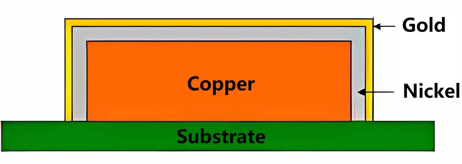
ENIG involves depositing a layer of electroless nickel, typically 3 to 7 micrometers thick, over exposed copper followed by a thin immersion gold layer of 0.05 to 0.23 micrometers. The nickel acts as a diffusion barrier, preventing copper migration, while the gold ensures oxidation-free solderability and electrical contact. This dual-layer structure contributes to ENIG thermal performance by maintaining pad integrity under thermal cycling. In high power PCBs, where components generate significant heat, surface finishes like ENIG influence solder joint reliability during reflow and operation. Poor thermal management exacerbates issues like black pad syndrome in ENIG, where nickel corrosion compromises joint strength and heat transfer. Thus, ENIG proves essential for applications demanding consistent ENIG heat dissipation, such as automotive electronics and telecommunications.
The relevance of ENIG in thermal contexts stems from its stability at elevated temperatures. Nickel withstands soldering peaks above 260 degrees Celsius without degrading, supporting lead-free processes common in high power designs. Gold's high conductivity minimizes contact resistance, aiding lateral heat spreading across pads. Engineers prioritize ENIG for high power PCBs because it offers a flat surface for fine-pitch components, reducing voids that could impede heat flow through joints. Industry standards like IPC-2221 emphasize heat dissipation in board design, underscoring the need to select finishes compatible with thermal demands. Overall, ENIG enhances system reliability by preserving thermal pathways over the board's lifecycle.
Technical Principles of ENIG Thermal Conductivity and Resistance
Heat dissipation in PCBs occurs primarily through conduction via copper traces and planes, convection from surfaces, and radiation, with surface finishes playing a subtle role in pad-level transfer. ENIG thermal conductivity derives from its materials: nickel at approximately 90 W/mK and gold at around 300 W/mK, though their thin profiles limit bulk impact. The nickel layer introduces a minor thermal barrier compared to direct copper exposure, but this effect diminishes in multilayer boards dominated by internal copper pours. Thermal resistance at ENIG-finished pads arises from interface resistances in solder joints, where gold promotes wetting and minimizes intermetallic formation that could hinder phonon transport. Engineers model these using Fourier's law, where heat flux q equals thermal conductivity k times temperature gradient over thickness. For ENIG, the gold-nickel stack adds negligible resistance in series with the substrate's lower conductivity, typically 0.3 to 0.5 W/mK for FR-4.
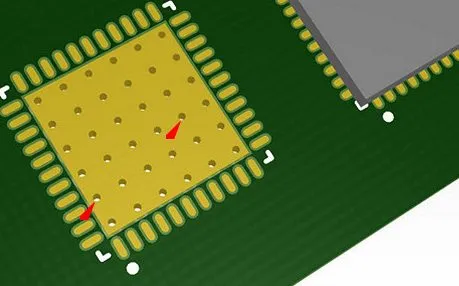
ENIG heat dissipation excels in scenarios with localized hotspots, as the uniform nickel-phosphorus alloy (7 to 11 percent phosphorus) provides consistent thermal diffusion. Medium-phosphorus nickel balances hardness and ductility, resisting cracking under thermal stress that could create voids and increase localized thermal resistance. In high power PCBs, ENIG thermal performance supports via-in-pad designs, where heat funnels through plated vias without finish-induced bottlenecks. Gold's low resistivity ensures efficient current flow, indirectly aiding Joule heating distribution. However, excessive nickel thickness can elevate through-plane resistance, prompting specs to cap it per IPC-4552 guidelines for ENIG plating. These principles guide simulations in tools like finite element analysis, predicting temperature rises under load.
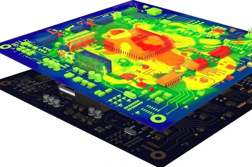
Evaluating ENIG thermal resistance involves junction-to-board metrics, where the finish affects the board-level path. JEDEC standards outline thermal characterization, highlighting how surface finishes influence package-to-board interfaces. In practice, ENIG outperforms thicker finishes in joint-level dissipation due to its planarity, reducing air gaps. Nickel corrosion, if unmanaged, raises resistance by disrupting metallic continuity, emphasizing process control. Engineers quantify this via infrared thermography, observing hotspot uniformity across ENIG pads versus alternatives.
Methods for Evaluating ENIG Heat Dissipation Performance
To assess ENIG thermal performance rigorously, engineers employ steady-state and transient thermal analysis per established protocols. Infrared imaging captures real-time dissipation during powered operation, revealing ENIG pad temperature profiles under high current. Thermal resistance testing measures theta-jb (junction-to-board), isolating finish contributions by comparing bare copper prototypes. Finite element models incorporate ENIG layer properties, simulating heat spreading from QFN packages on high power PCBs. Compliance with IPC-2221 ensures designs account for ambient conditions and airflow. These methods confirm ENIG suitability for densities exceeding 10 W per square centimeter.
Transient thermal analysis, using structure functions, deconvolves ENIG interface effects from substrate dominance. Pulse heating quantifies spreading resistance, where ENIG's flatness yields lower values than uneven finishes. For high power PCBs, accelerated life testing cycles boards from -40 to 125 degrees Celsius, monitoring joint degradation via shear strength. Acoustic microscopy detects voids impacting ENIG heat dissipation post-reflow. Data logging thermocouples on pads validates models, guiding iterations.
Best Practices for ENIG in High Power PCB Thermal Management
Selecting ENIG for high power PCBs requires specifying nickel thickness between 4 and 5 micrometers to optimize ENIG thermal resistance without excess barrier effect. Pair it with heavy copper (2 oz or more) and filled vias for vertical conduction paths. Embed thermal vias under hotspots, tented with ENIG to prevent solder wicking while preserving heat flow. Use high-Tg laminates (Tg above 170 degrees Celsius) compatible with ENIG processing temperatures around 80 degrees Celsius. Simulate early, incorporating ENIG material libraries for accurate ENIG thermal conductivity predictions. Factory controls per IPC-4552 mitigate phosphorus variability affecting ductility and thermal stability.
Design copper-balanced stackups to minimize warpage, ensuring uniform ENIG deposition. For ENIG heat dissipation, expose ground planes under components, leveraging gold's conductivity. Avoid over-etching, which thins nickel and compromises barrier function under heat. Post-plating bake stabilizes phosphorus content, enhancing cycle resistance. In assembly, profile reflow to stay below nickel's phosphor-induced degradation threshold. These practices elevate ENIG thermal performance in demanding environments.
Troubleshooting Common ENIG Thermal Issues
Engineers encounter ENIG-specific thermal challenges like hypercorrosion, where immersion gold attacks nickel, forming resistive compounds. Symptoms include elevated pad temperatures during testing, confirmed by cross-section analysis. Mitigation involves pH-controlled plating baths and minimum gold thickness. Black pad manifests as non-wetting areas post-reflow, increasing joint thermal resistance; SEM inspection reveals phosphorus-rich corrosion. Adjust electroless nickel chemistry to 8 to 9 percent phosphorus for balance. Thermal cycling reveals microcracks in thick nickel, spiking resistance; spec thinner layers for high power PCBs.
In high power scenarios, ENIG delamination from CTE mismatch causes hotspot migration. Adhesion promoters and controlled plating rates prevent this. Monitor via plating integrity, as thin ENIG there amplifies resistance. Data from JEDEC thermal tests guide thresholds. Systematic root cause analysis ensures reliable ENIG heat dissipation.
Conclusion
ENIG stands out for its balanced contribution to thermal management in PCBs, offering reliable heat dissipation through material stability and joint integrity. Key factors like controlled layer thicknesses and process adherence directly impact ENIG thermal performance, resistance, conductivity, and suitability for high power PCBs. By integrating standards-guided evaluation and best practices, engineers achieve optimal temperature control and longevity. Future designs will leverage ENIG's strengths alongside advanced substrates for even higher densities. Prioritizing these elements ensures robust, efficient boards.
FAQs
Q1: How does ENIG thermal conductivity compare to other finishes in high power PCBs?
A1: ENIG leverages nickel's moderate conductivity and gold's high value for efficient pad-level heat spreading, with minimal added resistance due to thin layers. It suits high power PCBs by maintaining joint integrity under load, outperforming uneven finishes in simulations. Factory processes per IPC-4552 ensure consistent properties. Overall, ENIG thermal conductivity supports reliable dissipation without dominating stackup thermal paths.
Q2: What factors influence ENIG heat dissipation performance?
A2: Layer uniformity, phosphorus content, and reflow profiling primarily govern ENIG heat dissipation. Nickel thickness affects barrier resistance, while gold prevents oxidation for sustained paths. In high power PCBs, thermal vias enhance it further. Standards like IPC-2221 guide integration for balanced designs.
Q3: Is ENIG suitable for applications requiring low thermal resistance?
A3: Yes, ENIG delivers low thermal resistance at solder interfaces thanks to excellent wetting and flatness, ideal for high power PCBs. Its stability under cycling minimizes degradation. JEDEC methods confirm performance in package-board paths.
Q4: How to test ENIG thermal performance in PCBs?
A4: Use IR thermography and transient analysis to measure dissipation and resistance. Power components to steady-state, logging pad temperatures. Cross-reference with models incorporating ENIG properties for high power validation.
References
IPC-2221B — Generic Standard on Printed Board Design. IPC.
IPC-4552 — Performance Specification for Electroless Nickel Immersion Gold (ENIG) Plating for Printed Boards. IPC.
JEDEC JESD51-2A — Integrated Circuits Thermal Test Method for Low Effective Thermal Resistance Junction-to-Case. JEDEC.


