 ALLPCB


Introduction
Double-layer printed circuit boards form a cornerstone in modern automotive electronics, offering a cost-effective solution for applications ranging from sensor interfaces to control modules. These boards feature conductive copper layers on both sides of a dielectric substrate, enabling more complex routing than single-layer designs while keeping manufacturing expenses lower than multilayer alternatives. In the demanding automotive environment, where systems must withstand extreme temperatures, constant vibration, and electrical stresses, automotive PCB design prioritizes reliability to prevent failures that could compromise vehicle safety. Double layer PCB auto configurations excel in non-critical subsystems like lighting controls, dashboard displays, and basic power management units. Engineers must balance performance needs with PCB reliability factors, ensuring compliance with rigorous qualification criteria. This article explores key design principles and reliability strategies tailored for electric engineers working on automotive projects.
What Are Double-Layer PCBs and Why They Matter in Automotive Applications
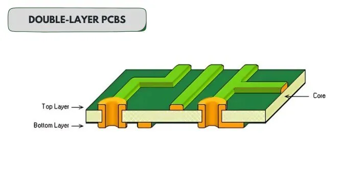
A double-layer PCB consists of two copper foil layers separated by a core material, typically FR4 laminate, with plated through-holes serving as vias to interconnect circuits across layers. This structure allows components to mount on both sides, doubling the available routing space compared to single-sided boards. In automotive electronics, double-layer designs suit applications requiring moderate complexity, such as engine control peripherals or infotainment interfaces, where high-density interconnects prove unnecessary. Their importance stems from the automotive sector's push for cost optimization amid rising electrification demands, yet without sacrificing durability under harsh conditions like road vibrations and thermal cycling. PCB reliability becomes paramount, as failures in these boards can lead to intermittent signals or complete system shutdowns. Selecting double layer PCB auto options thus requires engineers to evaluate trade-offs in signal integrity against multilayer boards.
Core Design Principles for Automotive PCB Design
Effective automotive PCB design begins with stackup definition, where the standard 1.6 mm board thickness accommodates most through-hole and surface-mount components used in vehicle systems. Copper weight, often 1 oz per square foot, supports current-carrying capacities typical in automotive power distribution circuits. Trace widths and spacings must account for voltage drops and creepage distances, guided by established design rules to prevent shorts under thermal expansion. Vias demand sufficient annular rings to maintain barrel integrity during plating and soldering processes. Signal routing separates high-speed lines from power traces to minimize crosstalk, while ground planes on one layer enhance return paths and reduce electromagnetic interference. Adherence to IPC-2221 provides a structured framework for these parameters, ensuring mechanical and electrical robustness.
Layer assignment plays a critical role, with one side often dedicated to analog signals and the other to digital or power sections for noise isolation. Thermal vias under power components transfer heat to the opposite layer, mitigating hotspots in confined automotive enclosures. Component placement follows logical flow from input to output, grouping heat-generating devices near board edges for chassis heat sinking. Engineers simulate impedance for controlled lines using field solvers integrated into layout tools, targeting 50 ohms for common automotive buses. These practices elevate double layer PCB auto performance without escalating to costlier multilayer stacks.

Key Reliability Factors in Double Layer PCB Auto Environments
Automotive applications expose PCBs to thermal cycling from -40°C to 125°C, inducing coefficient of thermal expansion mismatches between copper and substrate materials. This stress concentrates at vias and solder joints, potentially causing cracks over time. Vibration from engines and road surfaces accelerates fatigue in plated through-holes, where cyclic loading leads to barrel cracking if drill aspect ratios exceed recommended limits. Humidity ingress promotes dendritic growth across clearances, underscoring the need for robust surface finishes like HASL or ENIG. Mechanical shock during crashes or pothole impacts tests board warpage resistance, influenced by core thickness uniformity. PCB reliability hinges on proactive design to extend mean time between failures beyond 10 years.
Material selection favors high glass transition temperature laminates to resist delamination under solder reflow peaks. Solder mask thickness and via tenting prevent contamination during assembly. Conformal coatings add protection against salt spray in underbody modules. Qualification per IPC-6012 verifies performance through accelerated life tests simulating field conditions. These measures ensure double-layer boards meet automotive electronics durability expectations.
Best Practices for Enhancing PCB Reliability in Design and Fabrication
Start with symmetric copper distribution to minimize warpage during lamination and reflow, critical for double-layer boards lacking inner plane balancing. Wide power traces and pours reduce resistive heating, while stitching vias tie ground layers for uniform potential. Incorporate test points for in-circuit verification without compromising trace integrity. Fabrication tolerances tighten clearances to 0.15 mm minimum for high-volume automotive production. Assembly processes emphasize low-stress soldering profiles to preserve via reliability under vibration.
For signal integrity in automotive PCB design, route critical nets away from board edges prone to flexing. Use filled vias for high-current paths to boost thermal conductivity. Post-fabrication inspections check for voids in plating per IPC-A-600 criteria, flagging potential weak points early. Environmental sealing via potting complements design efforts in exposed locations. These best practices fortify double layer PCB auto against real-world stressors.
Common Challenges and Engineering Solutions
One prevalent issue in double layer PCB auto is via failure from thermal-mechanical fatigue, addressed by limiting via diameters to 0.3 mm and ensuring land-to-hole ratios exceed 2:1. EMI challenges arise from lacking dedicated shield layers, countered by perimeter ground fencing and ferrite beads on inputs. Poor thermal dissipation concentrates heat in ICs, resolved through copper-balanced layouts and multi-via arrays. Warpage exceeds 0.75% in thin boards, prompting thicker cores or constrained baking pre-assembly. Troubleshooting involves finite element analysis for stress prediction during design reviews.
Engineers mitigate humidity effects with edge plating or sealed enclosures, extending operational life. Iterative prototyping validates solutions under simulated automotive profiles. These targeted fixes maintain PCB reliability without multilayer complexity.
Conclusion
Double-layer PCBs deliver essential value in automotive applications through optimized automotive PCB design that prioritizes cost and simplicity alongside PCB reliability. Key principles like precise stackup, routing discipline, and material choices, informed by standards such as IPC-2221 and IPC-6012, enable robust performance under extreme conditions. Best practices in thermal management, vibration resistance, and fabrication controls further enhance longevity. Electric engineers benefit from these structured approaches to deploy reliable double layer PCB auto solutions in diverse vehicle systems. Ultimately, mastering these elements ensures electronics contribute to safer, more efficient automobiles.
FAQs
Q1: What are the primary design considerations for automotive PCB design using double-layer boards?
A1: Automotive PCB design for double-layer boards focuses on trace widths for current handling, via reliability under vibration, and thermal vias for heat spreading. Separate power and signal layers minimize noise, while high-Tg FR4 resists delamination. Compliance with IPC-2221 guidelines ensures mechanical integrity. These steps balance density needs with PCB reliability in harsh environments.
Q2: How does PCB reliability impact double layer PCB auto performance?
A2: PCB reliability in double layer PCB auto applications prevents failures from thermal cycling and shock, extending service life to match vehicle warranties. Design features like annular rings and conformal coatings combat fatigue and corrosion. Testing per IPC-6012 qualifies boards for automotive electronics stresses. Robust reliability supports consistent operation in engine bays or dashboards.
Q3: Why choose double-layer over multilayer for certain automotive electronics?
A3: Double-layer PCBs suit cost-sensitive automotive electronics like sensors where routing complexity stays moderate. They offer faster prototyping and lower fabrication costs without sacrificing basic signal integrity. Multilayer proves essential for high-speed buses, but double layer PCB auto excels in reliability for simpler modules. Proper design maintains performance parity in targeted uses.
Q4: What role do standards play in double layer PCB auto reliability?
A4: Standards like IPC-A-600 define acceptability criteria for plating and solder masks, ensuring double layer PCB auto withstands vibration and humidity. They guide inspections to catch defects early, bolstering overall PCB reliability. Consistent application across designs yields predictable field performance in automotive electronics.
References
IPC-2221B — Generic Standard on Printed Board Design. IPC.
IPC-6012E — Qualification and Performance Specification for Rigid Printed Boards. IPC, 2017.
IPC-A-600K — Acceptability of Printed Boards. IPC, 2020.


