 ALLPCB


Introduction
Single-layer PCBs offer a straightforward solution for electronic hobbyists tackling basic circuits like LED drivers or sensor boards. These boards feature components and traces on one side only, simplifying fabrication and reducing costs compared to multi-layer designs. Eagle CAD stands out as a free PCB software option that empowers users to create professional single layer PCB Eagle CAD layouts without steep learning curves. This Eagle CAD tutorial guides you through the entire process, from setup to output files ready for manufacturing. By following these steps, hobbyists can prototype custom designs efficiently. Whether you're building a prototype for a hobby project or experimenting with electronics, mastering single sided PCB layout Eagle unlocks creative possibilities.
What Is a Single-Layer PCB and Why Use Eagle CAD?
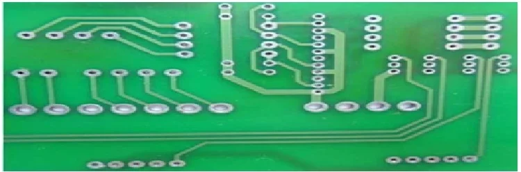
A single-layer PCB, also known as a single-sided board, confines all conductive traces, pads, and components to one copper-clad surface, typically the top side. The opposite side remains bare or covered with solder mask for protection. This design suits low-complexity circuits where signal integrity demands are minimal, avoiding the crosstalk issues common in denser multi-layer boards. Hobbyists favor single-layer PCBs for their ease of home etching or low-volume production, making them perfect for educational projects or proof-of-concepts.
Eagle CAD excels as PCB design software due to its intuitive interface and robust free version, which supports unlimited single-layer boards up to certain size limits. It provides essential tools like schematic capture, board layout, and autorouting tailored for single layer PCB Eagle CAD workflows. Unlike more complex alternatives, Eagle balances accessibility with precision, allowing hobbyists to enforce design rules that align with industry practices. Choosing Eagle CAD for single sided PCB layout Eagle ensures compatibility with standard manufacturing formats like Gerber files. Its library management and DRC (Design Rule Check) features help prevent common errors early in the process.
Understanding the Technical Principles of Single-Layer Design
In single-layer PCB design, traces must navigate around components without vias, relying solely on surface routing. This constraint demands careful component placement to minimize trace lengths and avoid overlaps, preserving signal quality in analog or low-frequency digital circuits. Copper thickness, usually 1 oz per square foot, dictates current-carrying capacity, calculated via width formulas to prevent overheating. Adhering to IPC-2221 guidelines for trace spacing and width ensures reliability under typical hobbyist operating conditions.
Thermal management poses another key principle, as heat dissipates primarily through the board and air. Hobbyists should position heat-generating components near edges for better convection. Solder mask application over traces reduces oxidation and shorts, while silkscreen layers add labels for assembly ease. Ground planes, if used, occupy unused copper areas to lower impedance, but require isolated routing to prevent shorts.
Fabrication tolerances influence design choices, with minimum trace widths around 0.006 inches feasible for professional runs. Eagle CAD's grid system aids precise placement, snapping elements to manufacturable increments. Understanding these mechanisms allows hobbyists to iterate designs confidently within the free PCB software environment.
Setting Up Eagle CAD for Your Single-Layer Project
Begin by downloading and installing the free version of Eagle CAD from its official source, ensuring compatibility with your operating system. Launch the software and create a new project folder to organize schematics and board files systematically. Select the "Board" editor from the project tree, setting dimensions to match your circuit needs, such as 50mm x 70mm for compact hobby boards. Configure layers to use only the top signal layer (layer 1), disabling bottom copper to enforce single-layer constraints.
Load standard libraries for common components like resistors, capacitors, and ICs via the library manager. Customize design rules under the DRC menu, setting clearance to 0.008 inches and minimum trace width to 0.010 inches for hobbyist-friendly fabrication. Enable ratsnest lines to visualize connectivity before routing. This setup phase in the Eagle CAD tutorial prepares a clean canvas for efficient single sided PCB layout Eagle.
Step-by-Step Guide to Designing Your Single-Layer PCB in Eagle CAD
Step 1: Create the Schematic
Switch to the schematic editor and place components from the library onto the sheet. Connect them with nets using the wire tool, labeling power rails like VCC and GND clearly. Run the Electrical Rule Check (ERC) to flag unconnected pins or duplicate references. Annotate components automatically for consistent numbering. Generate the netlist by running the "Generate/Switch to Board" command, transferring connectivity to the layout.
This schematic-first approach ensures logical flow before physical placement, a best practice in PCB design software.
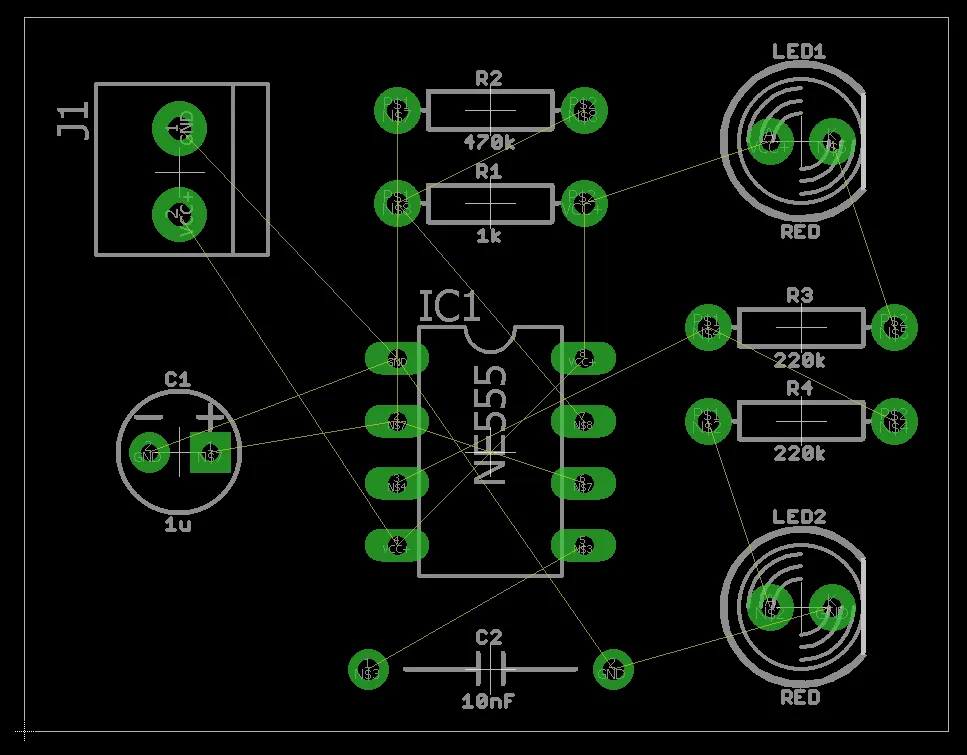
Step 2: Place Components on the Board
In the board editor, components appear as unplaced blocks; use the "Move" tool to position them intuitively, grouping analog and digital sections apart. Rotate elements with right-click for optimal orientation, minimizing trace crossovers. Invoke the ratsnest to display airwires guiding routing paths. Lock placed parts to avoid accidental shifts. For single layer PCB Eagle CAD, prioritize perimeter placement for connectors.
Step 3: Route Traces Manually or with Autorouter
Select the Route tool, choosing layer 1 and appropriate width from the DRC settings. Follow airwires to connect pads, bending traces at 45-degree angles to reduce reflections. Avoid right angles near sensitive traces. For complex nets, employ the Autorouter cautiously, reviewing paths for single-layer feasibility. Rip up and reroute as needed, ensuring no overlaps.
Manual routing fosters understanding of single sided PCB layout Eagle constraints, enhancing design skills.
Step 4: Add Text, Dimensions, and Finalize Layers
Place silkscreen text for labels using the Text tool on layer 21 (tPlace). Add mounting holes via the Hole tool on layer 17 (Dimension). Apply a solder mask outline on layer 29 (bMask) and top solder stop on layer 30 (tStop). Run a full DRC to verify clearances, widths, and shorts per IPC-A-600 criteria for board acceptability.
Step 5: Generate Manufacturing Files
Use the CAM Processor to output Gerber files for each layer: top copper (layer 1), mask (layer 30), silkscreen (layer 21), and drill files. Include a board outline on layer 20 (Dimension). Export a PDF for visual review. These files prepare your single layer PCB Eagle CAD design for etching or professional fab houses.
Best Practices for Reliable Single-Layer PCBs
Maintain trace separation exceeding 0.010 inches to mitigate arcing risks, aligning with IPC-2221 trace spacing recommendations. Use 10-20 mil widths for signal traces and wider for power paths. Incorporate test points on critical nets for debugging. For hobby etching, enlarge pads slightly to ease alignment. Simulate circuits in external tools if available, validating before layout.
Optimize board shape for mechanical stability, avoiding sharp corners that stress during handling. Document your design with notes in the schematic for future revisions. These practices elevate hobby projects to production quality within free PCB software limits.
Common Troubleshooting Tips for Eagle CAD Users
If DRC reports clearance violations, zoom into flagged areas and widen gaps or reposition elements. Autorouter failures on single-layer boards often stem from poor placement; manual intervention resolves most cases. Missing library parts require downloading user-contributed packages compatible with Eagle. Slow performance on large boards benefits from increasing memory allocation in the config file.
Ghosted traces indicate layer mismatches; confirm all routing on layer 1. For Gerber issues, verify CAM jobs match layer names precisely. These fixes streamline the Eagle CAD tutorial workflow.
Conclusion
Mastering single layer PCB Eagle CAD design through this step-by-step Eagle CAD tutorial equips hobbyists with skills for endless projects. From schematic to Gerber, Eagle CAD's tools deliver precise single sided PCB layout Eagle outcomes affordably. Prioritizing standards like IPC guidelines ensures durable results. Experiment iteratively, refining layouts for your unique needs. This free PCB software democratizes PCB design, fostering innovation in electronics hobbies.
FAQs
Q1: What makes Eagle CAD ideal for single layer PCB Eagle CAD beginners?
A1: Eagle CAD's free version supports unlimited single-layer boards with an intuitive drag-and-drop interface. Its schematic-to-board flow prevents errors early, while DRC enforces manufacturable rules. Hobbyists appreciate the autorouter for quick starts and manual tools for fine control. Overall, it balances power and simplicity in PCB design software.
Q2: How do I set design rules for single sided PCB layout Eagle?
A2: Access the DRC dialog to define clearance, trace width, and drill sizes based on fab capabilities. Set minimums like 8 mil clearance for hobby standards. Run checks iteratively during routing. This ensures compliance without overcomplicating single-layer designs.
Q3: Can I use Eagle CAD for more than just single-layer PCBs?
A3: Yes, the free tier handles double-sided up to size limits, with paid upgrades for multi-layer. Start with single layer PCB Eagle CAD to build skills, then expand. Libraries and netlist features scale seamlessly.
Q4: What files do I need from this Eagle CAD tutorial for PCB fabrication?
A4: Generate Gerbers for top copper, mask, silkscreen, and drills, plus an outline Excellon file. Review with a Gerber viewer. These suffice for most services handling single sided PCB layout Eagle.
References
IPC-2221B — Generic Standard on Printed Board Design. IPC, 2009
IPC-A-600K — Acceptability of Printed Boards. IPC, 2020


