ALLPCB


Introduction
DIY PCB etching remains a cornerstone for electronic hobbyists eager to prototype circuits without relying on commercial services. The toner transfer method stands out for its simplicity and accessibility in a home lab setup. However, achieving finer line widths pushes the boundaries of this technique, enabling denser layouts for surface-mount components and compact designs. Hobbyists often grapple with the DIY PCB etching minimum trace width, typically limited by transfer quality and etching precision. This article explores practical strategies to enhance homemade PCB trace width control and boost toner transfer PCB resolution. By refining your process, you can produce boards suitable for more advanced projects right from your workbench.
Why Finer Trace Widths Matter in Home PCB Fabrication
Trace width defines the copper conductors that carry signals and power on a PCB, directly impacting circuit density and performance. Narrower traces allow for higher component packing, essential for modern hobbyist designs like microcontrollers or RF modules. In professional fabrication, minimum widths are governed by capabilities, but home etching introduces variables like toner adhesion and etchant undercutting. Aligning hobbyist results with IPC-A-600 acceptability criteria ensures reliable conductor integrity despite manual processes. Finer lines also reduce material use and board size, making prototypes more efficient. Ultimately, mastering this skill elevates DIY efforts from basic through-hole boards to sophisticated layouts.
Technical Principles Behind Toner Transfer Resolution
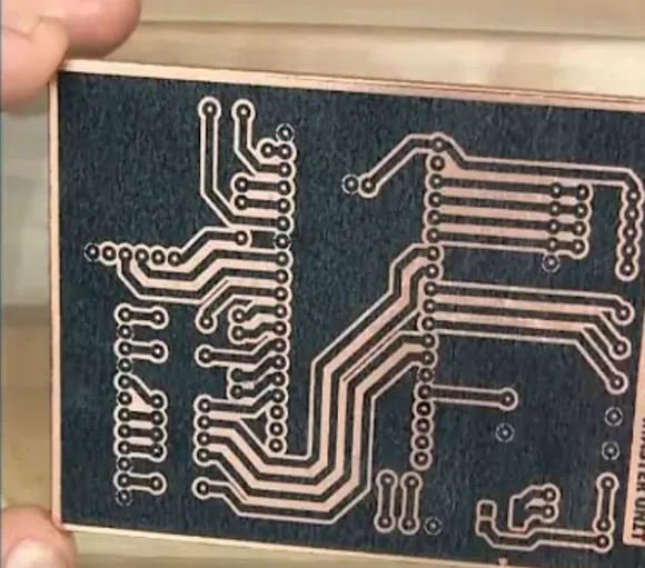
Toner transfer relies on laser printer toner acting as an etchant resist, transferred via heat and pressure onto clean copper-clad laminate. The resolution hinges on toner particle size, printer dot-per-inch rating, and transfer fidelity, where gaps in coverage lead to widened or bridged traces. During etching, the etchant attacks exposed copper laterally, causing undercutting that effectively increases the minimum trace width beyond design intent. Factors like copper surface preparation and etchant agitation influence this etch factor, typically around 10 to 20 percent in home setups. Higher DPI printing, often 1200 or more, minimizes toner spread, while uniform heating prevents voids. Understanding these mechanisms allows hobbyists to predict and compensate for resolution limits inherent to the process.
IPC-2221 provides guidelines on conductor spacing and width to maintain electrical integrity, principles that hobbyists can adapt for design rules. Poor transfer results in toner lifting, exacerbating undercutting and reducing effective toner transfer PCB resolution.
Factors Limiting DIY PCB Etching Minimum Trace Width
Surface contaminants on the copper foil repel toner, leading to incomplete coverage and broader effective trace widths after etching. Printer toner quality varies, with finer particles yielding sharper edges compared to coarser office-grade supplies. Heat application must balance adhesion without scorching, as excessive temperature causes toner flow and blurring. Paper choice affects release; glossy or magazine pages provide smooth transfer media that peels cleanly without fiber residue. Etchant chemistry, such as ferric chloride concentration, dictates attack rates, where fresh solutions minimize lateral etch. These combined factors often cap homemade PCB trace width at coarser dimensions unless optimized systematically.
Best Practices for Enhancing Toner Transfer PCB Resolution
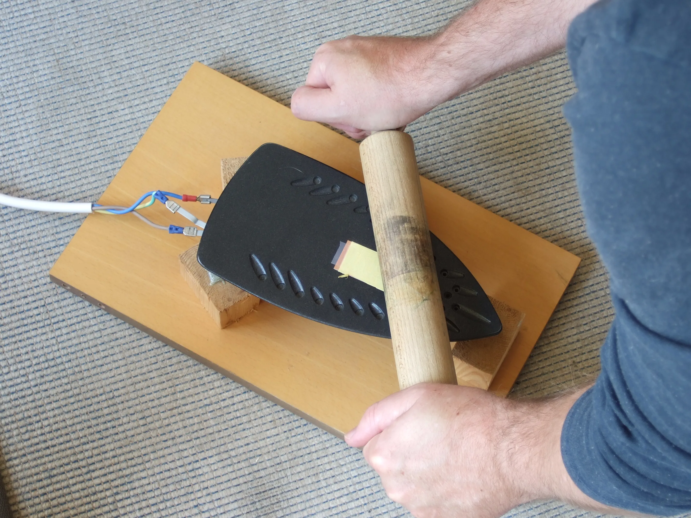
Start with meticulous copper preparation using a fine abrasive like Scotch-Brite pads followed by thorough rinsing and drying to ensure oxide-free surfaces. Select a high-resolution monochrome laser printer and print mirror-imaged layouts on glossy paper, such as inkjet photo sheets or magazine covers, at maximum DPI settings. Preheat the iron to cotton setting, apply firm pressure in circular motions for two to five minutes, and allow cooling before peeling the paper, sometimes after a brief water soak. For double-sided boards, align layers using registration holes and tape edges precisely before transfer. Post-transfer, inspect under magnification and touch up pinholes with a permanent marker. These steps consistently improve toner transfer PCB resolution, targeting sub-0.25 millimeter features with practice.
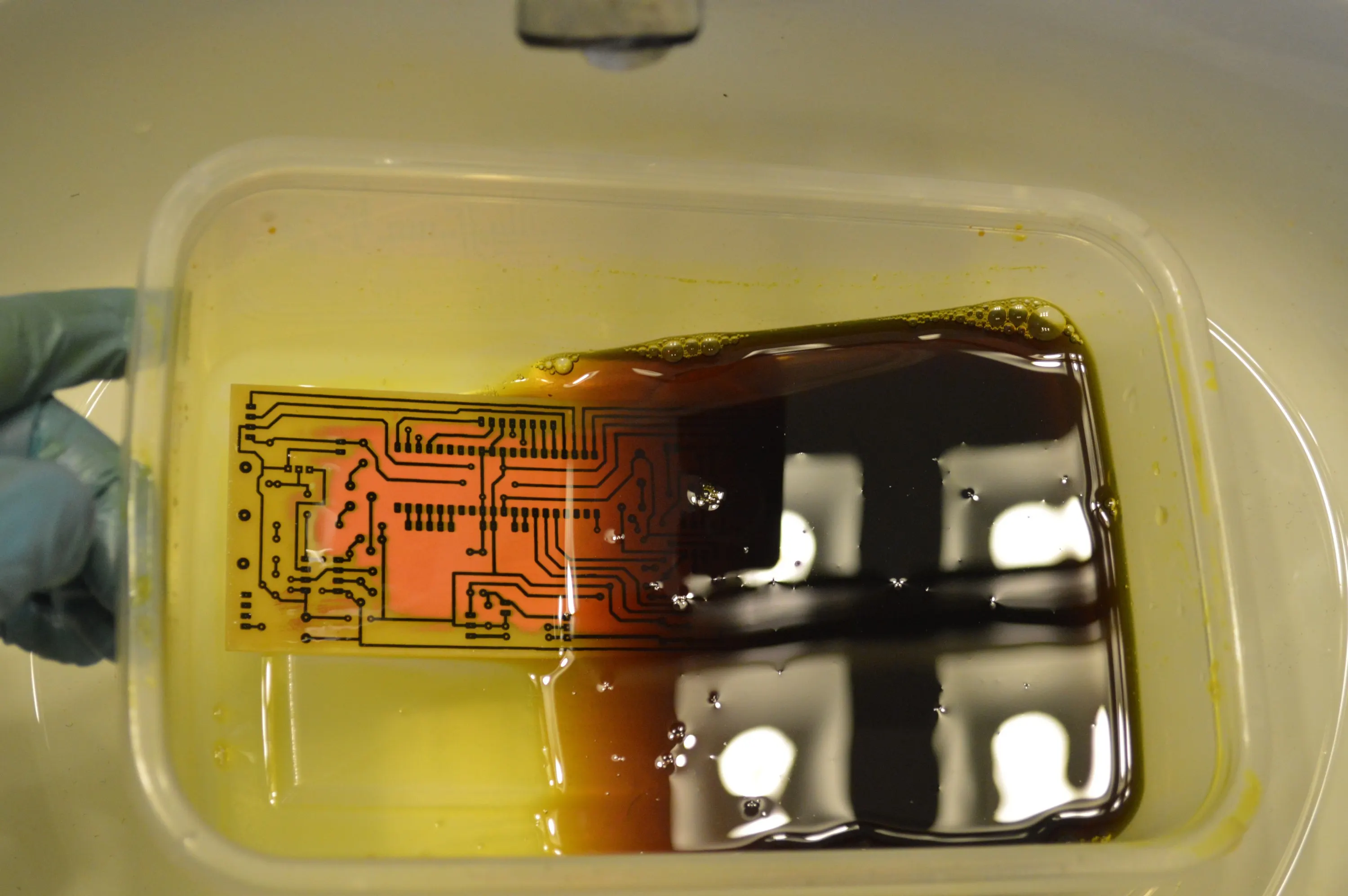
During etching, use a well-ventilated setup with bubbled ferric chloride at room temperature, agitating constantly to uniform etch rates and reduce undercutting. Rinse immediately in running water, then remove toner with acetone or sodium hydroxide soak. Design with IPC-6012 qualification specs in mind by adding etch compensation, widening traces by twice the expected copper thickness to account for fab tolerances. Test small panels first to dial in parameters for your setup.
Advanced Techniques for Subtle Finer Lines
Laminator machines offer superior pressure uniformity over irons, pressing toner deeper into copper for sharper delineations. Heat guns with vise clamping provide controlled reheating for stubborn areas, enhancing adhesion without distortion. Pre-etch toner hardening via oven baking at low temperatures strengthens resist integrity against aggressive etchants. For ultimate resolution, experiment with capacitor discharge transfer or hydraulic presses, though these demand more lab investment. Double-check artwork scaling and black fill density to avoid printer rasterization artifacts. Consistent calibration across these methods pushes DIY PCB etching minimum trace width toward professional thresholds.
Troubleshooting Common Issues in Homemade PCB Trace Width
Undercut traces often stem from prolonged etching or weak agitation, manifesting as narrowed conductors prone to opens. Toner voids appear from insufficient heat or dirty copper, bridgeable with resist pen but better prevented. Paper fibers clinging post-peel roughen edges, degrading resolution; acetone wipes or extended soaks resolve this. Overly aggressive ironing spreads toner, widening homemade PCB trace width; lighter passes suffice. Misalignment in multi-layer transfers causes shorts, fixable by precise fixturing. Systematic logging of variables like iron time and etchant strength accelerates process refinement.
Conclusion
Mastering finer line widths in DIY PCB etching transforms home labs into capable prototyping centers. Key lies in surface prep, precise transfer, controlled etching, and iterative testing aligned with standards like IPC-A-600. Hobbyists achieve reliable toner transfer PCB resolution through practice, enabling complex circuits without outsourcing. Experiment safely, document results, and scale designs confidently. This approach not only saves costs but builds deep process intuition for future innovations.
FAQs
Q1: What is the typical DIY PCB etching minimum trace width achievable at home?
A1: Many hobbyists reliably produce 0.25 millimeter traces with optimized toner transfer, starting broader at 0.5 millimeters for beginners. Finer 0.2 millimeter widths demand high-DPI printing, glossy paper, and precise ironing. Etch compensation in design counters undercutting. Consistent results follow from clean copper and fresh etchant, aligning hobby efforts with basic IPC tolerances. Practice on test strips refines your specific setup.
Q2: How can I improve homemade PCB trace width control during toner transfer?
A2: Prioritize copper scouring with non-metallic abrasives and immediate printing on glossy media. Apply even iron pressure for uniform adhesion, cooling fully before peel. Agitate etchant vigorously to minimize lateral attack. Touch up defects promptly and bake toner for durability. These yield sharper edges, reducing effective widths post-etch.
Q3: What factors most affect toner transfer PCB resolution in a home lab?
A3: Printer DPI, toner quality, and transfer pressure dominate, alongside copper cleanliness and paper type. Heat control prevents blurring, while etchant freshness limits undercutting. Design rules incorporating IPC-2221 spacing help predict outcomes. Testing incremental changes isolates variables for peak performance.
Q4: Why do traces widen after etching in DIY processes?
A4: Undercutting occurs as etchant penetrates resist edges, amplified by stagnation or aged solutions. Inadequate toner coverage from poor transfer exacerbates this. Compensate by widening artwork traces and using bubblers. Fresh ferric chloride and quick rinses preserve intended homemade PCB trace width.
References
IPC-6012E — Qualification and Performance Specification for Rigid Printed Boards. IPC, 2017
IPC-A-600K — Acceptability of Printed Boards. IPC, 2020
IPC-2221B — Generic Standard on Printed Board Design. IPC, 2003