 ALLPCB


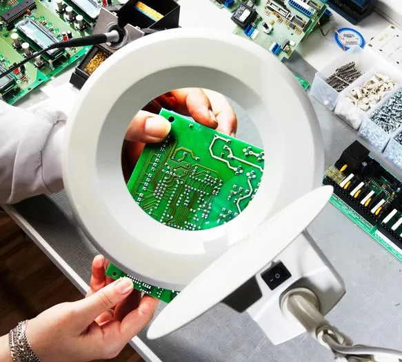
Introduction
Printed circuit boards, or PCBs, form the backbone of countless electronic devices, from hobby projects to everyday gadgets. When a PCB fails, many hobbyists face the choice between discarding it or attempting a repair. This DIY PCB repair at home guide walks beginners through the process, starting with visual inspection and culminating in soldering fixes. By following these steps, you gain hands-on skills that extend the life of your projects while saving costs. We cover identifying common PCB faults, essential tools for PCB repair, and safety precautions for PCB repair, all tailored for electronic hobbyists. Mastering these techniques builds confidence for more complex builds.
Why DIY PCB Repair at Home Matters for Hobbyists
Repairing PCBs yourself empowers hobbyists to troubleshoot and revive failed circuits without relying on professionals. It fosters a deeper understanding of electronics, turning trial-and-error into systematic problem-solving. For instance, fixing a simple fault like a cracked solder joint can restore functionality to an Arduino shield or drone controller. This approach aligns with industry practices outlined in standards like IPC-A-610J, which define acceptability criteria for electronic assemblies. Hobbyists benefit from cost savings and the satisfaction of self-reliance. Over time, these skills reduce waste and encourage sustainable electronics tinkering.
In the maker community, DIY repairs promote experimentation and learning from failures. You learn to spot patterns in faults, improving future designs. Professional services charge high fees for minor fixes, making home repair practical for budgets. It also prepares you for custom projects where replacements are unavailable. Embracing PCB repair enhances creativity in areas like robotics or audio amplifiers.
Identifying Common PCB Faults
Common PCB faults often stem from mechanical stress, overheating, or manufacturing defects, making visual inspection the first step in any repair. Burnt components appear discolored or charred, with a distinct smell indicating overheated resistors or capacitors. Cracked or cold solder joints look dull and grainy, failing to form a smooth fillet shape as per soldering standards. Broken traces show visible lifts or fractures, especially near connectors prone to flexing. Corrosion manifests as green or white powdery residue on pads or pins from moisture exposure.
To identify these, use good lighting and magnification to scan the board methodically. Start from power input areas, as faults cluster there due to high current. Check for bulging capacitors, a sign of electrolyte failure from overvoltage. Warped boards indicate thermal mismatch issues. Following guidelines from IPC-A-610J helps classify these as acceptable or requiring rework. Document findings with photos for reference during repair.
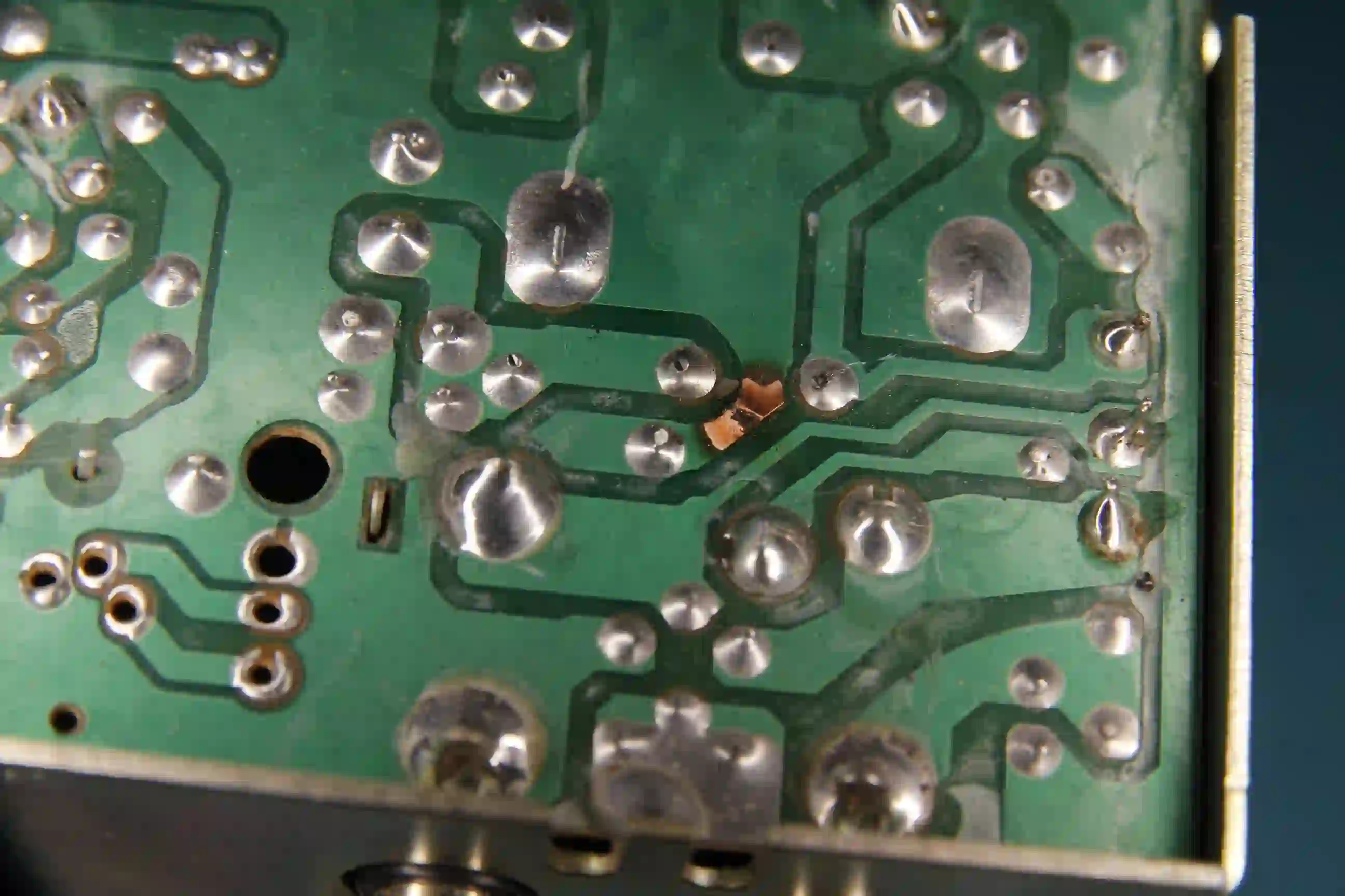
Other faults include bridged solder shorts, where excess material connects adjacent pads, causing unintended paths. Delaminated layers expose inner copper, often from improper storage. Mechanical damage like bent pins occurs from mishandling. Vias failing appear as dark rings or open circuits. Systematic inspection reveals 80 percent of issues without tools.
Essential Tools for PCB Repair
A basic toolkit enables effective DIY PCB repair at home for beginners. Start with a temperature-controlled soldering iron set to 300-350 degrees Celsius for most tasks. A digital multimeter measures continuity, voltage, and resistance to verify faults. Desoldering braid, wick, or a pump removes old solder cleanly. Flux pen improves solder flow and prevents oxidation.
Magnifying loupe or microscope aids precise inspection of fine-pitch components. Isopropyl alcohol and brushes clean residues post-repair. Helping hands clamp hold the board steady. Anti-static mat and wrist strap protect sensitive chips from electrostatic discharge. Tweezers and cutters handle small parts safely.
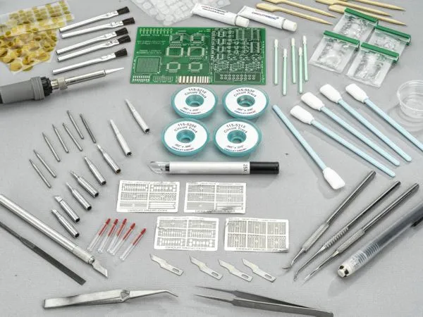
Optional additions like a hot air station suit surface-mount devices, but stick to basics initially. Quality tools last longer and yield better results. Store them organized to avoid loss. Invest gradually as skills grow.
Safety Precautions for PCB Repair
Safety comes first in PCB repair to prevent shocks, burns, or fumes inhalation. Unplug devices and discharge capacitors by shorting terminals with a resistor before handling. Wear eye protection against solder splatter and magnification for close work. Work in a ventilated area or use a fume extractor for lead-free solder vapors.
Ground yourself with an ESD wrist strap connected to the mat, as static zaps ruin ICs. Avoid touching pins with bare hands; use tools. Keep the workspace clutter-free to prevent slips. Handle batteries carefully to avoid shorts sparking fires. Follow these for incident-free sessions.
Heat components gradually to avoid lifting pads, per rework standards. Clean spills immediately. Have a fire extinguisher rated for electrical fires nearby. Train family on hazards if sharing space.
Step-by-Step Visual Inspection Guide
Begin visual inspection by powering off and inspecting the PCB under bright, angled light. Tilt the board to catch shadows revealing lifts or cracks. Check all solder joints for shine and shape: convex fillets indicate good bonds. Probe gently with a toothpick for loose parts. Note power plane discoloration signaling shorts.
Move to components: scan for physical damage like cracks in ceramic capacitors. Inspect connectors for bent pins or oxidation. Use the multimeter in continuity mode across traces, beeping for opens. Magnify BGA areas if applicable, though rare for hobby boards. Compare against IPC-A-610J criteria for class 2 assemblies suitable for consumer use.
Document with labels: "Fault: Burnt R10". Re-inspect after cleaning. This methodical approach pinpoints 90 percent of issues.
Beginner’s Guide to PCB Soldering and Repair Techniques
Soldering repairs follow IPC J-STD-001J principles for reliable joints. Clean the area with alcohol, apply flux to pads and leads. Heat the joint, not the iron tip on component, adding solder to melt into a cone. For through-hole, fill halfway, suck excess if needed. Surface-mount requires finer control, flowing solder around pads.
Desoldering starts with heating both sides, using wick to absorb molten solder. For stubborn parts, add flux and wick repeatedly. Lift gently with tweezers. Replace with matching component, observing polarity. Reflow new solder smoothly.
Practice on scrap boards first. Cool joints naturally. Clean flux residues. Test continuity post-repair.
IPC-7711/7721D details procedures for component removal and board repairs like trace fixes. Use jumper wires for broken traces, soldering ends securely. For lifted pads, scrape clean and bridge carefully.
Troubleshooting Tips for Common Issues
If power fails, check fuses or regulators first; burnt smells trace there. Noisy audio points to bad capacitors; replace electrolytics showing leaks. Intermittent faults suggest cracked joints from vibration; reflow them. Shorts beep on multimeter; isolate by removing parts sequentially.
For multilayer boards, faults hide inside; use schematics if available. Thermal imaging helps pros, but hobbyists rely on substitution. After repair, functional test under load. If fails, re-inspect.
Log repairs for patterns. Community forums share similar fixes, minus brands.
Conclusion
This guide equips electronic hobbyists with foundational skills for DIY PCB repair at home, from spotting faults to soldering fixes. Visual inspection reveals most issues quickly, while proper tools and safety ensure success. Adhering to standards like IPC J-STD-001J yields professional results. Practice builds proficiency, turning broken boards into working projects. Start small, stay patient, and enjoy the process.
Frequently Asked Questions
Q1: What are the most essential tools for PCB repair for beginners?
A1: Essential tools for PCB repair include a soldering iron, multimeter, desoldering wick, flux, and magnification. These cover 90 percent of home fixes for hobbyists. Start with quality basics to avoid frustration. A helping hands tool steadies work. This beginner's guide to PCB soldering emphasizes their role in reliable repairs.
Q2: How do I identify common PCB faults without advanced equipment?
A2: Identifying common PCB faults starts with visual checks for burns, cracks, or dull joints under light. Use a multimeter for continuity tests on traces. Clean first to spot corrosion. Follow IPC-A-610J for joint acceptability. Most faults show externally in hobby projects.
Q3: What safety precautions for PCB repair should hobbyists always follow?
A3: Safety precautions for PCB repair involve ESD protection, ventilation, eye gear, and discharging caps. Work unplugged, ground yourself, and use fume extraction. Avoid overheating to prevent pad damage. These steps prevent shocks, fires, and component loss in DIY settings.
Q4: Can beginners perform DIY PCB repair at home successfully?
A4: Yes, beginners succeed in DIY PCB repair at home with practice on scrap boards. Follow visual inspection to soldering steps methodically. Use flux for clean joints per standards. Patience resolves most faults like cold joints or bad caps. Build skills gradually.
References
IPC-A-610J — Acceptability of Electronic Assemblies. IPC, 2024
IPC-7711/7721D — Rework, Modification and Repair of Electronic Assemblies. IPC, 2024
IPC J-STD-001J — Requirements for Soldered Electrical and Electronic Assemblies. IPC, 2024


