ALLPCB


Introduction
In the fast-paced world of high-volume PCB assembly, panelization emerges as a critical step that bridges design and production efficiency. By combining multiple individual circuit boards into a single panel, manufacturers streamline processes like stencil printing, solder paste application, and pick-and-place operations essential for surface mount technology (SMT). A DFM-centric approach to panelization prioritizes manufacturability from the outset, minimizing defects such as component misalignment and board warpage that plague automated PCB assembly lines. This method ensures higher yields and faster throughput, particularly when scaling to thousands of units. Electrical engineers must grasp these optimization strategies to avoid costly rework and delays in production.
DFM-centric panelization goes beyond mere space-saving; it integrates precise fiducial marker placement, tooling hole optimization, and layout symmetry to align with the tolerances of automated equipment. Poorly planned panels lead to frequent machine stops, inaccurate placements, and increased scrap rates during SMT assembly DFM checks. Conversely, well-optimized panels enable seamless transitions through reflow soldering and inspection stages. As assembly lines demand ever-tighter precision, mastering these techniques becomes indispensable for reliable high-volume PCB assembly.
What Is DFM-Centric PCB Panelization?
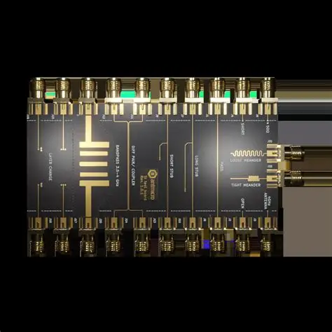
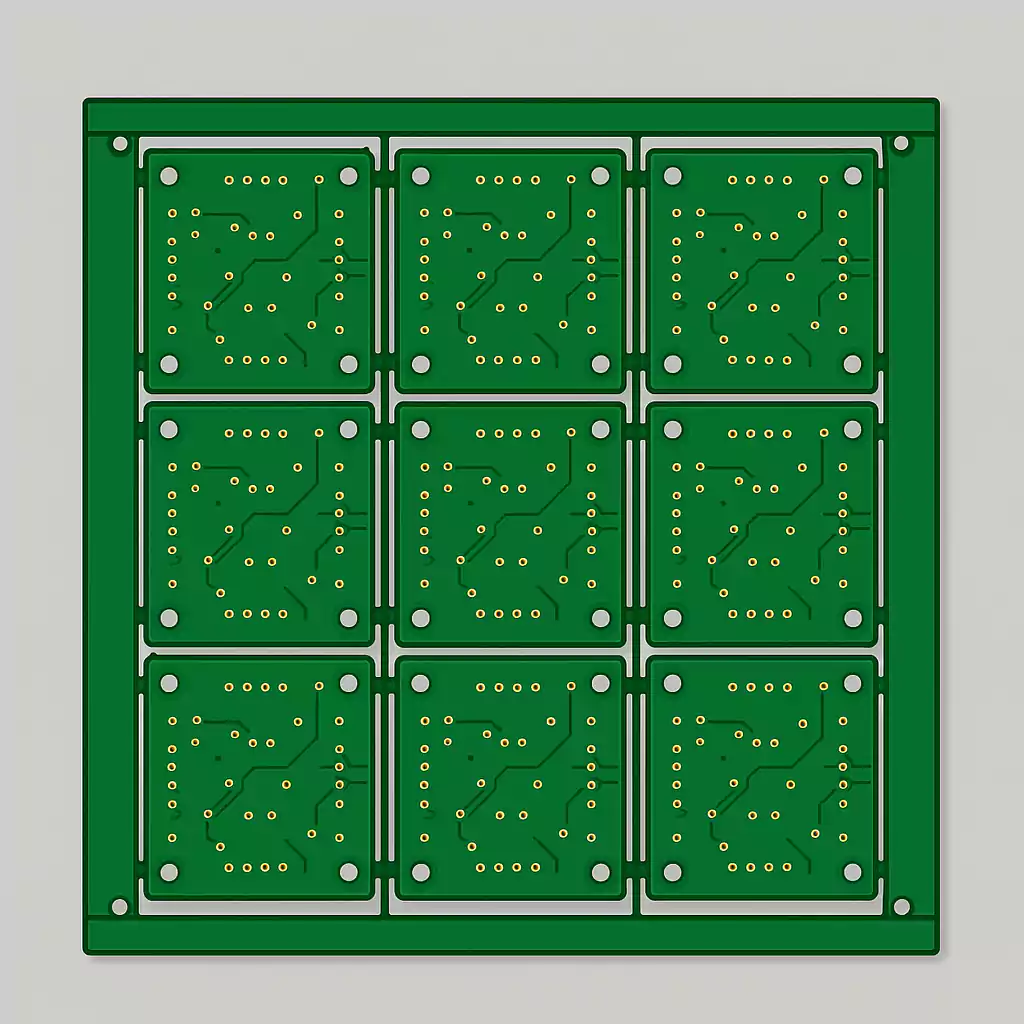
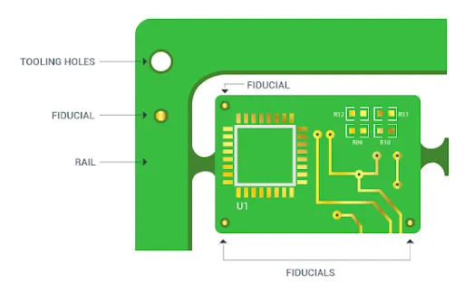
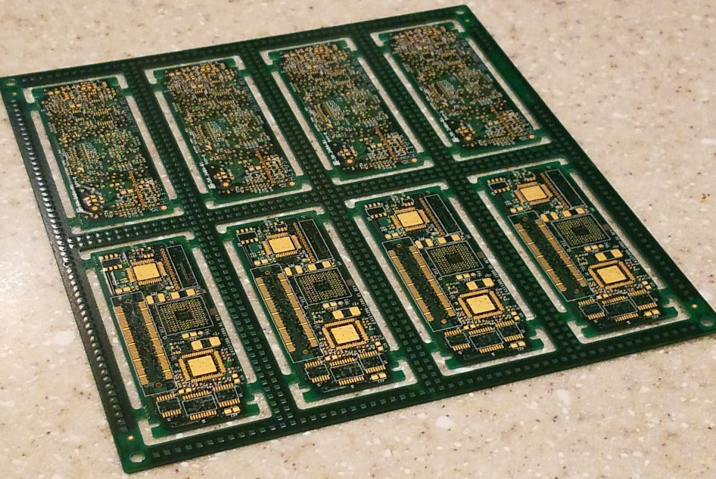
DFM-centric PCB panelization involves arranging multiple bare boards or assemblies into a larger panel format tailored specifically for automated manufacturing constraints. Unlike basic panelization, which focuses on fabrication economy, this approach incorporates assembly-specific features like fiducials and tooling holes to support pick-and-place machines and downstream processes. Panels typically feature outer rails for handling, breakaway tabs or V-scores for depaneling, and strategic cutouts to prevent mechanical stress.
The core goal is to create a unified substrate that automated PCB assembly equipment can process as one unit, reducing setup times and material waste. Engineers define panel dimensions based on equipment pallets, often around 300mm x 400mm or custom sizes up to 18x24 inches, while ensuring even distribution of boards to balance thermal and mechanical loads. This setup directly impacts SMT assembly DFM by facilitating consistent alignment across the entire array.
Key elements include global fiducials for initial machine vision calibration and local ones for fine-tuning on larger panels. Tooling holes provide mechanical registration for fixtures, stencils, and conveyors. Without these, variations in board position lead to tombstoning or bridging defects during reflow.
Why It Matters for Automated PCB Assembly
In high-volume PCB assembly, panelization dictates the rhythm of the production line, where pick-and-place optimization panelization can cut cycle times by grouping similar components for sequential placement. Automated systems thrive on predictability; misaligned panels force recalibrations, inflating costs and slowing output. Effective panelization ensures components stay within microns of target positions, critical for fine-pitch devices like 01005 passives or BGAs.
Component misalignment panelization issues arise from thermal expansion mismatches or handling vibrations, amplifying errors across multiple boards. Optimized layouts mitigate these by distributing mass evenly, preventing PCB warpage prevention panelization challenges during reflow ovens. Yield rates improve as inspection tools like AOI scan the entire panel uniformly, spotting defects early.
For electrical engineers, ignoring DFM in panelization means troubleshooting downstream failures, from skewed QFNs to shifted connectors. High-volume runs amplify these risks, turning minor oversights into major losses. Standards like IPC-A-610 emphasize visual and mechanical criteria that panel features directly support, ensuring assemblies meet class 2 or 3 reliability.
Technical Principles of Optimization
Fiducial Marker Placement
Fiducial markers serve as optical targets for pick-and-place cameras, enabling sub-micron alignment across the panel. Global fiducials, typically three per panel at corners or rail positions, establish the reference plane, while local fiducials handle dense or large-array corrections. Each marker consists of a 1mm diameter exposed copper pad with a 26mm clear zone free of solder mask, silkscreen, or nearby traces to avoid reflection errors.
Placement rules demand at least 5mm from panel edges and symmetric positioning to compensate for rotation or skew. In fiducial marker placement for SMT, asymmetry causes progressive misalignment, especially in high-volume PCB assembly where panels cycle repeatedly. Engineers must verify fiducials survive fabrication without oxidation or plating voids.
Tooling Hole Optimization
Tooling holes provide mechanical precision, pinning panels to conveyor pallets and aligning stencils with sub-0.1mm accuracy. Standard 3mm to 4mm non-plated holes, placed in pairs at opposite corners, accommodate pins without stressing the copper layers. Tooling hole optimization requires symmetry and spacing beyond 100mm apart to resist torque during handling.
In automated PCB assembly, mismatched holes lead to lateral shifts, propagating to component misalignment panelization. Holes must avoid inner board areas, residing solely on rails to preserve yield. Diameter tolerances under 0.1mm ensure repeatability across production runs.
Layout Strategies for Pick-and-Place Efficiency
Pick-and-place optimization panelization clusters components by feeder type, minimizing nozzle changes and head travel. Logical grouping, such as all 0805 resistors in one quadrant, boosts throughput by 20-30% in multi-head machines. Panel orientation aligns with machine axes, reducing theta errors.
Depaneling methods influence layout: V-scoring suits rectangular boards with straight edges, while tab-routing (mouse bites) handles irregular shapes but demands 3-5mm edge clearances for components. Rails, at least 10mm wide, host fiducials and barcodes without interfering with placement zones.
PCB Warpage Prevention in Panelization
PCB warpage prevention panelization counters CTE mismatches between copper and substrate during reflow peaks above 260°C. Asymmetric copper distribution or uneven board counts per panel induces bow up to 0.75% of diagonal, misaligning fine-pitch leads. Balanced layouts, with mirrored symmetry across axes, distribute stresses evenly.
Thicker panels or embedded stiffeners aid flatness, but core is uniform trace density and via placement. Per J-STD-001 requirements, warped panels exceed placement tolerances, causing opens or shorts. Engineers simulate warpage using panel symmetry checks early in design.
Best Practices for Implementation
Start with panel sizing matched to assembler pallets, maximizing board count without exceeding machine limits. Incorporate 10-15mm rails on all sides, adding two tooling holes per long edge and fiducials diagonally opposite. For SMT assembly DFM, enforce 5mm no-component zones from scoring lines to prevent damage during depaneling.
Group identical boards in arrays of 4-12, orienting them consistently for feeder efficiency in pick-and-place optimization panelization. Add local fiducials every 100-150mm on expansive panels to correct for minor warps. Verify layout with DFM software overlays simulating machine vision.
In high-volume PCB assembly, test panels with dummy runs to baseline alignment stats. Adjust for material effects, like FR-4 warpage in thick stacks. Document rail thickness matching depaneling tools, typically 1.6mm.
Troubleshooting Common Panelization Issues
Component misalignment often traces to fiducial occlusion by paste or debris; clean zones and polished surfaces resolve this. Warped panels from uneven cooling signal poor symmetry, fixed by redistributing ground planes. Tooling hole elongation from over-tight pins demands larger clearances or slotted designs.
In pick-and-place halts, check panel flatness against 0.5% bow limits; baking pre-assembly per IPC guidelines helps moisture-related warps. Mis-feeds link to rail flex; reinforce with thicker frames. Log defects to iterate layouts, targeting under 100ppm for high-volume.
Conclusion
DFM-centric PCB panelization transforms potential pitfalls into production strengths, optimizing fiducial marker placement, tooling hole optimization, and layouts for seamless automated PCB assembly. By prioritizing symmetry and clearances, engineers curb PCB warpage prevention panelization woes and component misalignment panelization risks. Adopting these practices elevates SMT assembly DFM, yielding robust high-volume PCB assembly outcomes. Consistent application ensures reliability from prototype to scale, aligning design intent with manufacturing reality.
FAQs
Q1: What role does fiducial marker placement play in pick-and-place optimization panelization?
A1: Fiducial markers provide reference points for machine vision systems, ensuring precise board alignment before component placement. At least three global fiducials per panel, symmetrically placed with clear zones, minimize errors in automated PCB assembly. Poor placement leads to cumulative shifts, but proper setup achieves sub-25 micron accuracy for high-volume runs. Troubleshooting involves verifying exposure and symmetry during DFM reviews.
Q2: How does tooling hole optimization prevent issues in SMT assembly DFM?
A2: Tooling holes secure panels mechanically for stencil alignment and conveyor transport, reducing lateral shifts during pick-and-place. Optimal 3mm non-plated holes in symmetric positions match fixture tolerances, avoiding stress on boards. In high-volume PCB assembly, misalignment from oversized or offset holes causes paste offsets; regular gauging maintains precision.
Q3: Why is PCB warpage prevention panelization critical for component misalignment panelization?
A3: Warpage from thermal stresses distorts fiducial positions, propagating misalignment across components in reflow. Balanced layouts and even board distribution keep bow below 0.75%, supporting SMT assembly DFM. Engineers prevent this by symmetrizing copper and using rails for stability in automated lines.
Q4: What are best practices for high-volume PCB assembly panel layouts?
A4: Maximize board count within pallet sizes, add 10mm rails with fiducials and tooling holes, and group components for feeder efficiency. Edge clearances of 5mm avoid depaneling damage, while V-scoring suits high throughput. Simulate warpage and alignment to refine designs upfront.
References
IPC-A-610H — Acceptability of Electronic Assemblies. IPC, 2020
J-STD-001GS — Requirements for Soldered Electrical and Electronic Assemblies. IPC/JEDEC, 2020
IPC-6012E — Qualification and Performance Specification for Rigid Printed Boards. IPC, 2017