 ALLPCB


Introduction
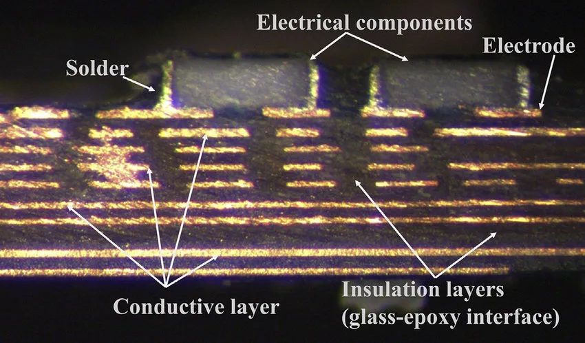
Multi-layer PCBs form the backbone of modern electronic systems where high component density and signal integrity demand stacked conductive layers separated by insulating materials. Delamination occurs when these layers lose adhesion and separate internally, creating voids that compromise electrical performance and mechanical stability. Engineers encounter this defect across aerospace, automotive, and telecommunications applications where reliability under thermal cycling and mechanical stress is essential. Understanding the mechanisms behind interlayer separation allows design teams to implement targeted controls from the initial layout stage through final assembly. This article examines the primary causes, diagnostic methods, and mitigation strategies for multi-layer PCB delamination while aligning with established industry practices.
What Is Delamination in Multi-Layer PCBs and Why It Matters
Delamination in multi-layer PCBs refers to the physical separation between adjacent conductive and dielectric layers, often initiated by moisture ingress, excessive thermal gradients, or residual stresses from fabrication. This internal defect differs from surface issues because it remains hidden until electrical testing or environmental exposure reveals intermittent opens or shorts. Industry relevance stems from its direct impact on product lifespan, with failures frequently appearing after repeated reflow cycles or field operation under varying humidity levels. Engineers must address multi-layer PCB delamination causes early because undetected separation can propagate into larger cracks that affect impedance control and power distribution. Preventing interlayer separation PCB issues supports consistent yield rates and reduces costly field returns in high-reliability sectors.
Technical Principles and Root Causes of Interlayer Separation
The fundamental mechanism involves breakdown of the bond between copper foil and prepreg or core materials, driven by differential expansion coefficients when the board experiences rapid temperature changes. Moisture absorbed during storage or processing converts to steam under reflow temperatures, generating internal pressure that forces layers apart. Poor surface preparation before lamination, such as inadequate oxide treatment or contamination, further weakens interfacial adhesion and creates initiation sites for separation. Thermal stresses accumulate during sequential lamination cycles in boards with eight or more layers, where inner layers experience prolonged heat exposure compared to outer layers. Material selection also plays a critical role, as certain resin systems exhibit higher moisture absorption rates that increase susceptibility to vapor pressure buildup. These combined factors explain why multi-layer PCB delamination causes often trace back to interactions between process parameters and material properties rather than a single isolated error.
Related Reading: Is Your Reflow Profile Sabotaging Your PCBs? Optimizing Soldering to Prevent Delamination
Diagnosing Delamination in Multi-Layer Boards
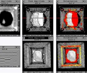
Effective diagnosis begins with non-destructive techniques such as acoustic microscopy, which detects voids and delaminated regions through reflected ultrasonic waves without damaging the board. Cross-sectional analysis follows for confirmation, revealing the exact location and extent of separation under high magnification. Engineers also monitor warpage and bow measurements after thermal excursions because excessive dimensional change frequently correlates with internal layer defects. Electrical testing can reveal symptoms indirectly through increased resistance or signal integrity degradation, though these indicators appear only after delamination has progressed. Systematic inspection protocols aligned with IPC-A-600K help standardize acceptance criteria and reduce subjective interpretation during quality reviews.
Practical Solutions and Best Practices for Preventing Delamination
Design teams reduce risk by specifying laminates with low moisture absorption and matching coefficients of thermal expansion across all layers to minimize internal stresses. Process controls during lamination include precise control of pressure, temperature ramp rates, and dwell times to ensure complete resin flow and void-free bonding. Moisture management protocols require baking boards at defined temperatures prior to reflow or assembly, following guidelines in JEDEC J-STD-020E for moisture sensitivity classification. Procurement specifications should mandate incoming material testing for resin content and glass transition temperature to verify consistency before production begins. During assembly, controlled reflow profiles with gradual heating and cooling phases limit peak thermal shock that could initiate separation. Post-fabrication handling procedures that avoid mechanical flexing or rapid environmental changes further protect against propagation of existing micro-voids.
Related Reading: Beyond FR-4: Choosing the Right PCB Laminate to Combat Delamination in Extreme Environments
Troubleshooting Insights for Engineers
When delamination appears in prototype builds, engineers first correlate failure locations with specific process steps such as inner-layer imaging or final press cycles. Reviewing stack-up symmetry and copper balance helps identify areas where unbalanced copper distribution may have induced warpage that contributed to separation. Adjusting prepreg resin flow characteristics or increasing oxide treatment dwell times often resolves adhesion issues in subsequent revisions. Documentation of all thermal profiles and material lot numbers enables traceability that accelerates root-cause identification across production lots. These structured troubleshooting steps support continuous improvement without requiring extensive equipment changes.
Conclusion
Delamination remains a manageable challenge in multi-layer PCBs when engineers apply systematic attention to material selection, process control, and inspection methods. Early identification of multi-layer PCB delamination causes through appropriate diagnostics prevents escalation into functional failures. Consistent application of industry standards such as IPC-6012E ensures that qualification requirements address adhesion and thermal performance from the outset. Implementing the outlined best practices reduces the incidence of interlayer separation PCB defects and supports reliable performance across demanding applications. Continued focus on these principles enables design and manufacturing teams to deliver robust boards that meet both performance and longevity expectations.
FAQs
Q1: What are the primary multi-layer PCB delamination causes during assembly?
A1: Moisture absorption combined with rapid thermal cycling during reflow represents the leading contributor, as trapped vapor expands and disrupts layer adhesion. Additional factors include insufficient oxide treatment on copper surfaces and unbalanced copper distribution that induces mechanical stress. Engineers mitigate these risks through controlled baking procedures and symmetric stack-up designs.
Q2: How does diagnosing delamination multi-layer boards differ from surface defect inspection?
A2: Diagnosis relies on non-destructive methods such as acoustic microscopy to detect internal voids, followed by targeted cross-sectioning for verification. Surface inspection alone cannot reveal hidden separation between internal layers. Standardized criteria from IPC-A-600K guide consistent evaluation across production batches.
Q3: What steps help in preventing delamination multi-layer PCBs in high-layer-count designs?
A3: Prevention starts with selecting low-moisture-absorption laminates and maintaining precise lamination parameters including pressure and temperature profiles. Pre-assembly baking according to established moisture sensitivity classifications removes absorbed water before thermal stress exposure. Symmetric copper distribution and controlled reflow profiles further minimize internal stresses that lead to separation.
Q4: How do internal layer defects affect long-term reliability of multi-layer PCBs?
A4: Internal separation creates pathways for moisture ingress and electrical discontinuities that may manifest only after extended field operation or repeated thermal cycles. These defects compromise signal integrity and increase the probability of intermittent failures. Early detection and process corrections maintain the mechanical and electrical integrity required for mission-critical applications.


